



Semiconductor laser soldering for chip packaging uses a focused diode-laser spot (commonly 915 nm or 976 nm) to reflow a pre-placed solder deposit — paste, preform, jetted ball or wire — in a localized, sub-second heatin…
Semiconductor laser soldering for chip packaging uses a focused diode-laser spot (commonly 915 nm or 976 nm) to reflow a pre-placed solder deposit — paste, preform, jetted ball or wire — in a localized, sub-second heating cycle, so the joint forms without running the whole package through a convection oven. The process is used for die attach on power and sensor packages, BGA/CSP ball attach and rework, cavity and lid-frame sealing pads, connector and lead-frame joints, and single-die repair where the surrounding material cannot take a second full reflow. What separates a repeatable laser soldering process from an unreliable one is not laser power alone but closed-loop temperature control at the joint, matched deposit geometry, and an inspection plan that catches voids and intermetallic growth before reliability testing does.
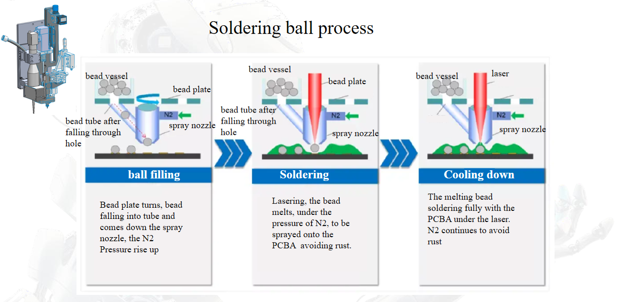
What does a laser soldering process flow look like in chip packaging?
A typical inline sequence for package-level laser soldering runs in six steps, and each step has a measurable acceptance gate:
- Pad preparation and flux/paste deposition. Stencil print, jet dispense or pin transfer. Solder paste volume repeatability should be held within ±10% for fine-pitch pads; flux-only processes need a deposit thin enough to volatilize inside the heating window rather than under the beam.
- Component or ball placement with vision alignment. CCD fiducial alignment typically holds ±10–25 µm at placement for pitches below 0.4 mm. Placement error larger than 25% of pad width is the most common cause of downstream bridging that gets misattributed to the laser.
- Nitrogen shielding. Oxygen concentration at the joint is normally held below 1,000 ppm, and below 500 ppm for SnAgCu alloys or for die attach where voiding targets are tight. Poor shielding shows up first as dull fillets and elevated void area, not as a temperature fault.
- Laser reflow with closed-loop temperature control. A pyrometer or thermopile samples the joint at 1–10 kHz and modulates diode current to follow a programmed profile — preheat, ramp, peak, time above liquidus, controlled cool-down.
- Controlled cooling. Natural or assisted cooling in nitrogen; forced air on thin die is a common source of CTE-driven cracking.
- Inspection and test. AOI for fillet geometry and placement, X-ray or CSAM for voids, shear/pull on sampled units, cross-section for intermetallic thickness on first article and after any parameter change.
Laser reflow, solder ball jetting or wire feeding — which fits your package?
The three delivery methods are not interchangeable; they differ in deposit size, pitch capability and how much heat reaches the part.
| Item | Solder paste + laser reflow | Laser solder ball jetting | Solder wire + laser |
|---|---|---|---|
| Typical deposit | 0.1–0.5 mm³ printed or dispensed | 80–760 µm ball diameter | 0.2–0.8 mm wire |
| Pitch capability | 0.2–0.5 mm | 0.3–0.8 mm | 0.5 mm and above |
| Deposit consistency | Dependent on print/dispense, ±10% | Ball diameter tolerance ±5–10 µm | Wire feed ±5% length |
| Typical use | Die attach, package pads, cavity sealing pads | BGA/CSP ball attach, bump repair, single-ball rework | Connectors, lead-frame tabs, shield and frame joints |
| Flux handling | Flux in paste; residue cleaning usually required | Flux-free or micro-flux; cleaner joints | Flux-cored or pre-applied flux |
| Heat input per joint | Lowest, beam absorbs into paste and pad | Low, ball melts in flight or on pad | Highest, wire must be fed and fused |
Selection rule of thumb: if the joint is defined by a printed pad and you need alloy flexibility, use paste plus laser reflow. If you need flux-free, single-ball placement at high positional accuracy — ball attach, rework, custom bumping — use jetting. If the joint is a through-hole, tab or connector termination where filler volume is large, wire feeding is the practical choice.
Which parameters actually control joint quality?
Laser power is the least useful number to specify, because it changes with spot size, absorptivity and fixture. Specify the thermal profile and the beam geometry instead, then let closed-loop control deliver the power.
| Parameter | Typical working range | Effect if out of range |
|---|---|---|
| Spot diameter at work surface | 0.3–2.0 mm, top-hat preferred | Too large: adjacent re-melt and die heating; too small: uneven fillet, cold joint at pad edge |
| Ramp rate | 100–300 °C/s | Too steep: spatter, flux burnout, die cracking; too slow: oxidation, extended cycle |
| Peak joint temperature | SAC305 240–250 °C; SnBi 175–185 °C; AuSn 300–330 °C | Low: cold joint, poor wetting; high: IMC growth, die stress |
| Time above liquidus | 0.5–2.0 s | Short: incomplete coalescence, voids; long: brittle IMC, grain coarsening |
| Temperature control | Closed loop at 1–10 kHz, ±3–5 °C repeatability | Open-loop power control drifts with pad finish and part absorptivity |
| Nitrogen O₂ at joint | <1,000 ppm; <500 ppm for tight void targets | Higher oxide fraction, dull fillets, void area increase |
Two practical notes from the line. First, always verify pyrometer readings against a contact thermocouple on the first article, and re-verify after any change of pad finish or solder alloy — emissivity differences between bare copper, ENIG and OSP can shift the indicated peak by 10–20 °C. Second, on thin die or warped substrates, the limiting factor is usually the temperature gradient across the part, not the peak. Reducing spot size and adding a short preheat hold typically fixes warpage-related opens better than lowering peak temperature.
How do you troubleshoot common laser soldering defects in packages?
| Symptom | Likely cause | Corrective action |
|---|---|---|
| Solder spatter / micro-balling | Ramp too steep, moisture in paste, flux burnout before melting | Reduce ramp to 100–150 °C/s, verify paste storage and expiry, add a 100–150 °C preheat hold |
| Void area above target in die attach | Trapped volatiles, insufficient time above liquidus, contaminated pad | Extend time above liquidus to 1.5–2 s, raise N₂ flow, check pad finish and cleanliness |
| Dull fillet, poor wetting | Peak temperature low, oxygen ingress, pyrometer offset | Compare thermocouple to pyrometer, raise peak 5–10 °C, leak-check the shielding nozzle |
| Die crack or delamination after reflow | Cooling too fast, spot larger than the die, excessive gradient | Slow cool-down, shrink spot, add preheat, check die thickness against power density |
| Adjacent joint re-melted | Spot overlap, sequence too fast for heat to dissipate | Reduce spot or power, increase joint-to-joint delay, re-sequence from centre outward |
| Ball diameter variation in jetting | Nozzle wear, inconsistent ball feed, misaligned landing | Nozzle maintenance interval, feed audit, re-teach vision offset |
What acceptance checks should follow laser soldering?
- First-article thermal verification: thermocouple profile at the joint, compared against the pyrometer trace, documented before production release.
- Fillet and placement AOI: fillet height and wetting angle within drawing limits, no bridging, no tombstoning, placement within 25% of pad width.
- Void inspection by X-ray or CSAM: single-digit void percentage for power die attach is a common target; BGA joints are usually accepted below 25% void area per ball, tighter for thermal pads.
- Mechanical sampling: die shear or ball shear and pull per the applicable JEDEC or MIL-STD method, with limits set from your own baseline rather than a generic figure.
- Cross-section on change control: intermetallic compound thickness typically held in the 0.5–2 µm range for Cu-Sn systems; excessive IMC is a sign of too much heat, not too little.
- Electrical test and, where relevant, thermal cycling on the qualification lot.
FAQ
Is laser soldering the same as laser welding?
No. Soldering melts a filler alloy below roughly 450 °C and does not melt the base metal; welding fuses the base metal itself. They use different optics, different shielding and completely different quality criteria, so a welding recipe should never be transferred to a soldering application.
Can laser soldering replace oven reflow in chip packaging?
Not across the board. Convection and IR reflow remain more economical for high-volume boards with uniform thermal mass. Laser soldering wins where heat must be localized: heat-sensitive sensors and optical packages, sequential ball attach, single-die rework, and high-mix lines where oven profiling per product is impractical.
Why are 915 nm and 976 nm diode wavelengths common?
They are mature, fiber-deliverable, and economically available at the power levels needed for sub-second reflow, with absorptivity in solder paste and metal pads high enough to reach melting without excessive power. 1064 nm sources are also used where tighter focus or different absorption is required.
How is joint temperature controlled without contact?
A pyrometer or thermopile measures the joint spot and the controller modulates diode current at 1–10 kHz to follow the programmed profile. Accuracy depends on emissivity calibration against a thermocouple, so recalibrate whenever alloy, pad finish or component material changes.
What package types are a poor fit for laser soldering?
Large-area thermal pads needing uniform heating over more than a few millimetres, and parts with tall components that shadow the beam, are usually better served by conventional reflow or vapour phase.
If you can share your package type, pad finish, alloy and void target, our engineers will help you map these parameters onto a laser soldering configuration and outline the acceptance checks to run first.