


Semiconductor laser soldering is a non-contact, localized soldering process in which a diode laser (typically 915 nm or 980 nm, fiber- or direct-coupled) delivers energy to a defined spot, heating only the joint area to …
Semiconductor laser soldering is a non-contact, localized soldering process in which a diode laser (typically 915 nm or 980 nm, fiber- or direct-coupled) delivers energy to a defined spot, heating only the joint area to melt solder ball, paste, or wire while the rest of the board and package stay near ambient. Its defining characteristics are high ramp rates (100–400 °C/s), millisecond-scale dwell times (50–800 ms), tight closed-loop peak-temperature control (±5–10 °C via pyrometer feedback), and a very small heat-affected zone — which is what makes it suitable for fine-pitch connectors, sensor packages, optical modules, and thermally sensitive semiconductor assemblies that cannot survive a full reflow profile.
Why does laser soldering behave differently from reflow or iron soldering in semiconductor packaging?
The heat transfer mechanism is the root of most process differences. Reflow heats the whole assembly through convection; a soldering iron heats through conduction from a tip in contact with the joint. Laser soldering heats by absorbing photons in the top few hundred nanometres of the solder and pad finish, then conducting inward. Three consequences follow, and each has a practical implication:
- Heating is surface-down and asymmetric. The solder and pad finish absorb first; the component lead and the die side heat by conduction. Joints with large copper planes underneath need noticeably more energy than the same joint on a thin trace, so power settings are not transferable between board designs — they must be re-quantified per pad stack.
- Reflectivity matters as much as power. Bare SnAgCu reflects a significant share of near-infrared energy; ENIG, oxidized copper, and fluxes with dark residues absorb more. A pad finish change from ENIG to bare OSP can shift the required energy by a noticeable margin, so absorptivity should be treated as a process variable, not a constant.
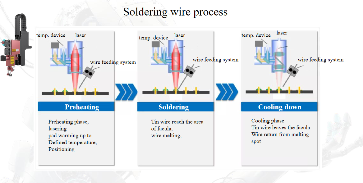
- Thermal mass is small, so control must be fast. Because the heated volume is tiny, temperature rises and falls in tens of milliseconds. Open-loop power control produces wide part-to-part variation; closed-loop control using a pyrometer or two-colour sensor sampled at kHz rates is what holds peak temperature repeatably.
Note that this is a soldering process — solder melts and wets a metallization to form an intermetallic joint. It is not laser welding, where base metal is fused; no melting of the copper, lead frame, or substrate occurs in a correctly set laser soldering process.
What is the practical process window for laser soldering semiconductor devices?
The table below shows ranges that hold across typical SAC305 and low-temperature SnBi assemblies. Treat them as starting points for a design-of-experiments, not as fixed recipes.
| Parameter | Typical range | Practical notes |
|---|---|---|
| Laser wavelength | 915 nm / 980 nm diode; 1070 nm fiber | Shorter wavelengths are absorbed better by solder and Cu; 1070 nm suits larger spots and deeper joints |
| Spot diameter at work plane | 0.3–2.0 mm | Match to joint footprint; oversized spots damage adjacent passives and wire bonds |
| Output power (CW) | 5–120 W | Small ball joints at the low end; connector pins and thermal pads at the high end |
| Ramp rate | 100–400 °C/s | Fast enough to limit IMC growth, slow enough to avoid flux spatter |
| Dwell above liquidus | 50–800 ms | SAC305 (217 °C): 240–260 °C peak, 30–50 °C above liquidus |
| Cooling rate | 50–150 °C/s | Fine grain, less warpage; too fast can crack brittle SnBi joints |
| Nitrogen purity | <1000 ppm O₂, 100–500 ppm preferred | Reduces oxides, improves wetting on OSP and bare Cu |
| Filler form | Ball 0.15–0.76 mm; wire 0.1–0.4 mm; paste Type 4–6 | Ball feeding gives the most repeatable volume for fine-pitch joints |
Which semiconductor and electronics assemblies actually benefit?
Laser soldering earns its cost where three conditions overlap: the joint is small, the surrounding area cannot take reflow-level heat, and the assembly is expensive enough to justify per-joint monitoring. In practice that means:
- Automotive electronics: ECU connector pins, current-sense shunts, sensor terminals, and wire-to-pad terminations where the housing or a nearby component limits total heat exposure.
- Semiconductor packaging: solder-ball attachment to package pads, lid and frame sealing on hermetic packages, MEMS and image-sensor modules where die-level thermal budget is tight.
- Optical modules: TO-can and butterfly package joints, flex-to-package connections — thermal drift during soldering directly affects alignment.
- Rework and single-joint repair: replacing one connector or BGA-adjacent component on a populated, high-value board without disturbing neighbouring joints.
- Medical device electronics: fine-wire and sensor connections where the surrounding polymer or coating has a low degradation temperature.
Where it fits less well: large-area joints with heavy copper planes, high-volume simple boards where a reflow oven is cheaper per unit, and joints hidden under a component body where the beam cannot reach.
What are the common failure symptoms and how do you troubleshoot them?
| Symptom | Likely cause | Action |
|---|---|---|
| Dull, grainy, incomplete wetting | Energy too low, dwell too short, heavy local heat sinking | Verify actual peak temperature with a thermocouple or calibrated pyrometer; lengthen dwell before raising power |
| Solder spatter / micro-balls | Ramp too fast, flux outgassing, moisture in paste | Add a 20–50 ms preheat step; check paste storage and thaw procedure |
| Voiding above 15% by X-ray | Insufficient flux activation, poor N₂ coverage, oxidized paste | Improve nozzle placement; confirm O₂ reading at the joint, not at the chamber inlet |
| Pad cratering, dielectric discoloration | Spot too small with high power, energy concentrated on thin dielectric | Increase spot diameter and reduce power; check beam profile is top-hat, not hot-centred |
| Bridging between fine-pitch leads | Excess paste or ball volume, spot overlap onto neighbouring pad | Reduce deposit volume 10–20%; re-check vision alignment offset |
| Die or package micro-cracks | Cooling too fast with CTE mismatch, or excessive peak temperature | Reduce cooling rate; cap peak at 30–40 °C above liquidus |
How do you verify the process is in control?
Build acceptance around measurable outputs rather than machine settings:
- Intermetallic layer: cross-section and measure the Cu₆Sn₅ layer; 1–3 µm continuous is a healthy SAC305 joint. Below 1 µm suggests incomplete melting; above 5 µm signals excessive time above liquidus and a brittle joint.
- Void rate: X-ray or CT; typically <5% for thermal-path joints and <10–25% for general signal joints, per your product spec.
- Wetting angle: below 30° on pad and lead, assessed visually or by AOI.
- Mechanical strength: ball shear or wire pull on first-article and periodic samples; track the mean and standard deviation, not just the pass/fail limit, so drift shows up early.
- Temperature trace logging: record every joint’s pyrometer curve. A shift in the curve’s shape usually precedes a visible defect by hours of production.
FAQ
Is laser soldering the same as laser welding?
No. Soldering melts filler metal at 180–260 °C to wet a metallization; welding fuses base metal, typically above 1000 °C. Laser soldering leaves the copper, lead frame, and substrate unmetled, which is why it suits heat-sensitive packages.
Can one laser setup handle both 0.2 mm solder balls and connector pins?
Usually not with the same optics. Ball joints need a 0.3–0.6 mm spot with fast, low-energy pulses; connector pins need 1–2 mm spots and far more energy. Plan for interchangeable optics or a dual-head configuration.
How important is nitrogen?
Noticeable for OSP and bare-copper finishes, less so for ENIG with a good flux. Below roughly 1000 ppm O₂ at the joint, wetting becomes consistent; verify with a measurement at the work zone rather than at the gas inlet.
Does laser soldering reduce thermal damage to nearby components?
Yes, because the heat-affected zone stays close to the spot — typically a few hundred micrometres — so parts a few millimetres away see only a brief, small temperature rise. This is measured, not assumed: confirm with thermocouples on the nearest sensitive component during first-article qualification.
How long does process development take for a new board?
For a single joint type, a design-of-experiments covering power, dwell, and spot size typically converges within a few dozen builds, followed by first-article cross-section and X-ray validation. Multi-joint boards take longer mainly because each pad stack needs its own energy setting.
If you are evaluating laser soldering for a semiconductor or automotive electronics assembly, send us your pad stack, solder alloy, and thermal constraints and we will help you define a starting process window.