


Choosing a suitable laser soldering process comes down to matching four things to the joint you actually have: the solder delivery format, the laser and optics configuration, the closed-loop temperature profile, and the …
Choosing a suitable laser soldering process comes down to matching four things to the joint you actually have: the solder delivery format, the laser and optics configuration, the closed-loop temperature profile, and the inspection criteria you will accept or reject against. When those four are aligned with joint geometry, thermal mass and your quality standard, the process repeats shift after shift; when any one is mismatched, you get cold joints, solder splash or pad damage that no amount of parameter tweaking will fix. Work through the sequence below before you commit to a machine configuration.
What Should You Define Before Choosing a Laser Soldering Process?
Start with a one-page joint requirements sheet rather than a machine specification. Most process failures we see in the field trace back to a requirement that was never written down — usually thermal mass or solder volume.
- Alloy and melting range. SAC305 reflows around 217–220 °C, Sn63Pb37 at 183 °C, and low-temperature SnBi alloys near 138 °C for heat-sensitive parts. The alloy sets your peak temperature window and your cooling constraints.
- Joint geometry. Pad length and width, lead or pin cross-section, the gap the solder must bridge, and the target fillet volume. A 0.4 mm pitch connector and a 2 mm through-hole pin need completely different optics.
- Thermal mass and heat path. Copper thickness, number of ground planes, whether the pad sits on a 4-layer board with a thermal relief or a solid plane. Heavy copper pulls heat away from the joint and is the single most common reason a profile that worked on the prototype fails in production.
- Board material and finish. FR4, BT, ceramic and flex substrates behave differently; ENIG, OSP and HASL surfaces change wetting and the time to first wetting.
- Quality standard. State it up front — IPC-A-610 Class 2 or Class 3, J-STD-001, plus any internal void limit measured by X-ray.
- Throughput and integration. Joints per second, inline or stand-alone, SMEMA handshake, and whether the same platform must handle rework.
Which Solder Delivery Format Matches Your Joint?
The feeder format decides your solder volume repeatability, your minimum feature size and your cycle time. Pick it against the joint, not against machine convenience.
| Format | Typical size range | Best suited to | Main constraint |
|---|---|---|---|
| Solder ball | 0.15–0.76 mm diameter | Fine-pitch connectors, BGA/CSP reball, micro joints with a defined volume | Ball placement accuracy; needs a matching nozzle and flux deposition step |
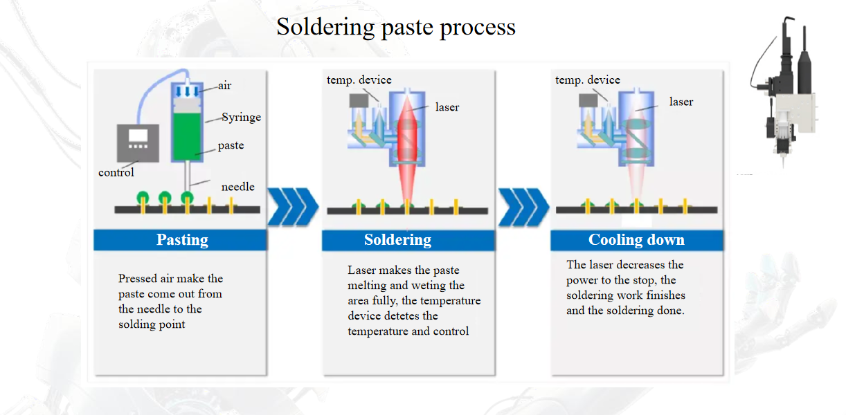
| Solder paste | Type 4–6 powder, 0.1–0.3 mm deposits | Fine-pitch leads, pad arrays, mixed-technology boards | Flux residue and slump; print or dispense volume control |
| Solder wire | 0.3–0.8 mm diameter | Through-hole pins, connector tails, larger terminals, rework | Wire feed resolution at small joints; contact force on the joint |
For a joint under roughly 0.3 mm, ball or paste is normally the only way to hold volume tolerance within ±10%. For a connector tail with 1 mm or more of exposed pin, wire feed is usually faster and easier to automate.
How Do You Size the Laser Spot and Power for the Joint?
The spot must cover the pad and lead with a small margin, and must not overlap the adjacent pad or a plastic housing. In practice this means a spot between roughly 0.3 mm and 3 mm, with the optical design chosen so the energy distribution matches the joint — a flat-top profile for pad arrays where you need even heating, a controlled Gaussian for a single pin where you want the centre to reach reflow first.
- Wavelength and absorption. Near-infrared sources around 808–980 nm and 1064 nm are the common choices for soldering. Bare copper reflects a large share of that energy at room temperature, which is why preheating the assembly — even to 80–120 °C — changes the process more than adding laser power does.
- Power density over total power. A joint that reflows in 0.8 s at 30 W over a 1 mm spot may burn at 30 W over a 0.4 mm spot. Always evaluate power density (W/mm²) against spot area, not the nameplate wattage.
- Pyrometer and control geometry. The temperature measurement spot must sit fully inside the laser spot and be filled by the joint. If the pyrometer averages the pad edge or the board surface, the closed loop chases the wrong temperature.
- Emissivity stability. Flux flowing across the measurement spot changes apparent temperature. Use a short-wavelength or two-colour measurement, and validate the reading against a thermocouple on the first articles.
- Vision alignment. CCD alignment in the ±25–50 µm range is typical for fine-pitch work; confirm the field of view covers your largest and smallest parts without a lens change.
How Do You Build a Repeatable Temperature Profile?
A laser soldering profile is short but still has distinct stages. The values below are working starting points for SAC305 on a typical FR4 assembly; tune them per joint with a design-of-experiments rather than one-factor-at-a-time.
| Stage | Typical setting | What it controls |
|---|---|---|
| Preheat | 80–120 °C, 1–3 s (or assembly-level preheat) | Reduces reflectivity, drives off solvent, limits thermal shock |
| Ramp to reflow | 100–250 °C/s at the joint | Wetting speed; too fast causes solder splash and flux spatter |
| Reflow dwell | Peak 235–250 °C, 0.5–3 s above liquidus | Fillet formation and intermetallic growth |
| Cooling | 2–6 °C/s, forced air or gas | Grain structure; slow cooling gives dull, coarse joints |
Store one profile per joint type rather than one per board. Closed-loop control with a sampling interval in the low milliseconds is what keeps a 1 s reflow stable when the board underneath varies. Where oxidation is a concern, nitrogen shielding at the nozzle with oxygen below about 1000 ppm improves wetting on OSP and bare-copper surfaces noticeably.
How Do You Qualify the Process and Read Failure Symptoms?
Qualification is a first-article exercise followed by a small DOE on the three variables that matter most: peak temperature, dwell time and solder volume. Accept the process when cross-sections show an intermetallic layer of roughly 1–4 µm, X-ray voiding is inside your stated limit, fillets meet the IPC class you selected, and pull or shear results sit comfortably above the minimum with a tight spread. Then run a capability check across at least three boards from different panel positions.
| Symptom | Likely cause | First action |
|---|---|---|
| Dull, grainy or cold-looking joint | Peak too low, dwell too short, or slow cooling | Raise peak 10 °C, extend dwell by 0.5 s, add forced cooling |
| Solder splash and beading | Ramp too fast, flux outgassing, contaminated surface | Lengthen preheat, reduce power density, check board cleanliness |
| Insufficient wetting on one side | Spot offset, uneven energy distribution, thermal shadow | Re-centre alignment, switch to flat-top optics, check heat path |
| Pad discolouration or laminate blister | Power density too high, spot overlapping board surface | Reduce power, tighten spot, shorten dwell |
| Excess voiding under the joint | Flux entrapment, contaminated finish, cooling too fast | Adjust preheat ramp, verify alloy and storage, slow final cooling |
FAQ
Can laser soldering replace reflow for a whole board? Not usually. It is strongest where selective heating wins: heat-sensitive components, thick copper or metal-core areas, connectors, and rework. Most lines run reflow for the bulk and laser for the joints that reflow handles poorly.
What laser power do I need for a 0.5 mm pitch connector? Power alone is not a useful specification. Define spot diameter first — typically 0.4–0.8 mm for that pitch — then find the power density that reaches reflow in your target cycle time. A 30–60 W source is common, but the delivered density at the joint is what matters.
How do I avoid damaging nearby plastic or a heat-sensitive part? Use the smallest spot that still covers the joint, keep the joint between the laser and the sensitive part where possible, add a gas shield or mask, and cap the peak with a closed-loop limit rather than relying on time alone.
Why does my joint look dull even though it passes X-ray? Dullness usually points to cooling rate or an alloy/finish interaction rather than a bad joint. Check cooling first, then confirm the pad finish and paste shelf life before changing the profile.
Is nitrogen always required? No. It becomes worthwhile when you are soldering onto OSP or bare copper, when dwell times are short, or when your void and wetting limits are tight. On ENIG with generous dwell, air soldering often meets Class 2.
If you send us your joint drawing, alloy and quality standard, we can help you narrow the delivery format, spot size and profile window before you specify a system.