


Laser soldering is a reflow process in which a focused laser beam — typically a 915 nm diode or 1070 nm fiber source — is used as the heat source to melt a pre-placed solder deposit (solder ball, solder paste or solder w…
Laser soldering is a reflow process in which a focused laser beam — typically a 915 nm diode or 1070 nm fiber source — is used as the heat source to melt a pre-placed solder deposit (solder ball, solder paste or solder wire) and form a metallurgical joint on an electronics assembly. Because energy is delivered optically and only where the beam lands, the heat-affected zone is usually limited to 1–3 mm around the joint, allowing a single joint to be reflowed in 0.5–3 s without subjecting the whole board to reflow oven temperatures. It is used in production where fine pitch, local rework, heat-sensitive neighbours or 3D/odd-form geometries make oven reflow or iron hand-soldering unreliable.
How does a laser soldering machine actually create a joint?
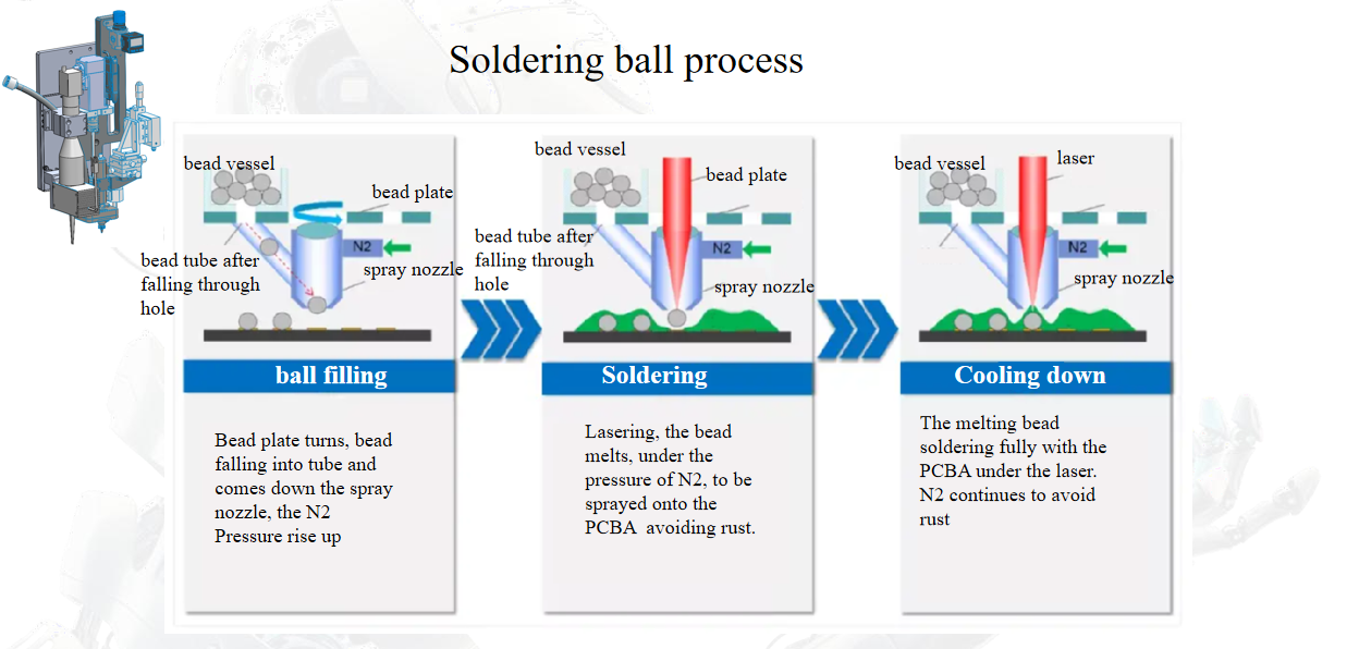
The sequence is the same on every platform we build, whether it is a stand-alone cell or an inline module:
- Deposition. A solder ball feeder drops a pre-formed sphere (0.2–1.2 mm) onto the pad, or a dispenser places paste / a wire feeder advances wire to the joint. Ball feeding gives the most repeatable volume; paste suits fine-pitch and multi-joint patterns.
- Alignment. Coaxial CCD vision locates the pad and the deposit, then offsets the beam path. Repeatability is typically ±10–25 µm, which is what makes 0.3 mm pads and 0.4 mm pitch connectors practical.
- Heating. The beam is focused to a 0.3–2.0 mm spot and the joint is ramped at 100–400 °C/s to peak. A pyrometer or two-colour sensor reads the joint temperature in real time and a closed-loop controller modulates laser output, so the profile is temperature-controlled rather than time-controlled.
- Solidification and inspection. Laser power cuts off, the joint freezes in 0.1–0.5 s, and post-solder AOI checks wetting, fillet shape, ball collapse and position before the part moves on.
Nitrogen shielding (≥99.99%, 5–20 L/min, O₂ typically held under 100 ppm at the joint) is common on fine-pitch and automotive work because it widens the wetting window and reduces dross on the nozzle.
What are the subsystems of a laser soldering system?
- Laser source and optics — diode or fiber laser, delivery fiber, collimator, focusing lens, and in multi-joint cells a galvo scanner to jump between joints without moving the part.
- Closed-loop thermal control — pyrometer feedback, per-joint profile library, and data logging of every joint’s peak temperature and time-above-liquidus for traceability.
- Solder delivery — ball feeder with diameter verification, paste dispenser with jet or time-pressure valves, or wire feeder.
- Vision and motion — CCD alignment camera, XY gantry or robot, force-controlled nozzle or hold-down to keep the deposit in contact with both surfaces during melting.
- Atmosphere and mechanics — N₂ nozzle, fume extraction, water or air cooling for the optics.
- Automation interface — SMEMA conveyor, MES/SECS-GEM links, recipe management, and AOI hand-off for inline lines.
Laser-based solder jetting: how it works and when to use it
Laser-based solder jetting is a non-contact method in which a focused beam melts solder inside a small nozzle and a short nitrogen pulse ejects the molten droplet onto the pad. Because the droplet leaves the nozzle already liquid, the joint never sees a contacting tool, and the deposit volume is fixed by the nozzle aperture, chamber pressure and pulse width instead of by contact time.
This is what separates jetting from laser wire soldering. With a wire, the filler touches the joint and the deposit grows with feed time; with jetting, each pulse delivers a repeatable droplet, so the same deposit can be placed thousands of times per hour on pads that a wire cannot reach. It is the practical choice for recessed or stacked joints, for parts that must not be touched during reflow, and for flex or thin-substrate assemblies where any mechanical load is a risk.
Jetting does not replace every wire or paste process. Large thermal masses and joints that need a fillet built up over several passes are still more economical with wire feeding, and fine-pitch SMT pads are usually served by paste. Jetting earns its place where access is difficult and repeatability matters more than deposit size.
| Aspect | Laser solder jetting | Laser wire soldering | Laser solder paste |
|---|---|---|---|
| Filler delivery | Non-contact droplet | Contact wire feed | Pre-printed or dispensed |
| Deposit control | Nozzle diameter and pulse width | Wire feed rate and dwell | Stencil aperture or dispense volume |
| Typical joint | Recessed, stacked, hard-to-reach | Terminals, through-hole, ground pads | Fine-pitch SMT, rework |
| Contact force | None | Light | None |
If your joint geometry is hard to reach or your cycle time target rules out contact dispensing, compare the options with our laser solder ball mounting process guide, the solder paste application guide and the wire feeding troubleshooting notes. Equipment configurations are listed on the laser soldering systems page.
Laser soldering vs. iron, hot-bar and selective wave — which process fits the joint?
| Process | Heat input / spot | Typical cycle per joint | Board thermal load | Best fit | Main limitation |
|---|---|---|---|---|---|
| Laser (ball / paste / wire) | 0.3–2.0 mm optical spot, 100–400 °C/s ramp | 0.5–3 s | Low; HAZ ~1–3 mm | Fine pitch, connectors, heat-sensitive neighbours, 3D and shield-frame joints | One joint at a time in most configurations; needs vision and profile development |
| Soldering iron / robot iron | Contact tip, 2–8 mm | 2–6 s | Medium–high, conducted | Rework, low volume, through-hole touch-up | Tip wear, operator dependence, pad damage risk |
| Hot-bar / pulse-heat | Thermode, entire row | 5–15 s per row | Medium–high | Flex-to-board, ACF bonding, connector rows | Thermode flatness and coplanarity; thermal expansion of flex |
| Selective wave | Molten wave, whole panel preheat | Batch / 20–60 s per pass | High, whole assembly | Through-hole and mixed-technology boards | Flux management, shadowing, not for SMD fine pitch |
What process parameters have to be set and verified?
| Parameter | Typical working range | What to verify |
|---|---|---|
| Laser power at the work surface | 10–120 W (30–60 W common for 0.4–0.76 mm balls) | Power meter check at focus; watch for lens contamination drift |
| Spot diameter | 0.3–2.0 mm; about 1.2–1.5× pad width | Burn-paper or beam-profiler measurement; too large a spot heats neighbours |
| Ramp rate | 100–400 °C/s | Fast ramp cuts oxidation but raises splatter risk |
| Preheat / soak | 100–150 °C for 0.3–1 s (flux activation) | Reduces voids and thermal shock on thick ground planes |
| Peak joint temperature | 210–240 °C for SAC305; 183–200 °C for SnPb | Measured with a fine thermocouple or calibrated pyrometer, not assumed from the recipe |
| Time above liquidus | 1–3 s | Long enough for IMC formation, short enough to limit brittle growth |
| N₂ flow / O₂ at joint | 5–20 L/min; <100 ppm O₂ | In-line O₂ analyser at the nozzle exit |
| Solder ball diameter | 0.2–1.2 mm | Volume consistency; a 0.05 mm diameter error is roughly 15% volume |
Acceptance is normally written against the drawing plus a standard: J-STD-001 and IPC-A-610 Class 2 or 3 for fillet and wetting, a wetting angle under roughly 30–45°, intermetallic layer of about 1–3 µm on cross-section, and voiding limits agreed by X-ray (commonly ≤25% of joint area for power and automotive joints, tighter for some RF and sensor parts). Confirm shear or pull strength on the first-off sample and after any paste, ball or pad-finish change — not once at machine buy-off.
What defects appear, and how do you troubleshoot them?
- Cold joint / dull, incomplete wetting. Raise peak temperature or extend time above liquidus by 0.5 s; check the spot is centred on the pad, not the lead; verify pad shelf life and O₂ level. Oxidised pads will not wet regardless of energy.
- Ball not collapsing, partial reflow. Energy is going into the surrounding copper rather than the joint — reduce spot size, add preheat, or confirm power at the surface with a meter.
- Splatter and solder beading. Ramp is too steep or flux is spitting; add a 0.3 s preheat, clean the nozzle, and check N₂ flow is not blowing molten solder off the pad.
- Voids above limit. Usually flux outgassing or moisture: bake the boards, check paste storage and thaw time, and slow the ramp through the flux-active window.
- Damage to adjacent parts. Spot overlaps a neighbour or a ground plane is sucking heat; shrink the spot, shorten dwell, or use a galvo cell with a tighter profile.
- Weak pull strength on cross-section. IMC under 0.5 µm means under-heating; over 4 µm of brittle intermetallic means over-heating. Adjust energy rather than force.
Which applications benefit most from laser soldering?
Automotive electronics is the largest driver: ECU boards with heavy copper planes, sensor and connector pins that sit next to plastic housings, and wiring harness joints where an iron cannot reach. Semiconductor packaging uses the same principle for fine-pitch lead frames, die-attach to heat-sensitive substrates, and shielding or lid attach where local heat protects the die. Optical modules, medical device electronics and miniaturised consumer boards follow, mainly because the low thermal load protects MEMS, crystals and thin-film sensors within a few millimetres of the joint.
FAQ
Is laser soldering the same as laser welding?
No. Soldering melts a filler alloy below roughly 450 °C and bonds it to the pad through a thin intermetallic layer; welding melts the base metal itself. They use different optics, power densities and joint design, and the acceptance criteria share nothing.
Can laser soldering replace reflow ovens?
For most high-volume SMD boards, no — oven reflow remains the efficient choice. Laser soldering wins on localised joints, heat-sensitive assemblies, mixed-technology boards, and rework of single joints without reflowing the whole panel.
Does the laser damage nearby components?
Not when the spot is sized correctly. Heat is confined to a 1–3 mm zone, and closed-loop temperature control cuts power once the setpoint is reached, so a 0402 capacitor 2 mm away typically sees far less heat than in an oven excursion.
How long does a recipe take to develop?
For a single joint type, expect one to two days of profiling and cross-sectioning; a board with several joint families typically takes one to two weeks including AOI tuning and first-article approval.
What maintenance does the head need?
Daily check of the protective window and nozzle, weekly power verification at the work surface, and periodic pyrometer calibration — contaminated optics are the most common cause of a recipe that “suddenly stops working”.
If you share your joint geometry, pad finish and throughput target, our process engineers can recommend a laser soldering configuration and profile starting point for your line.