


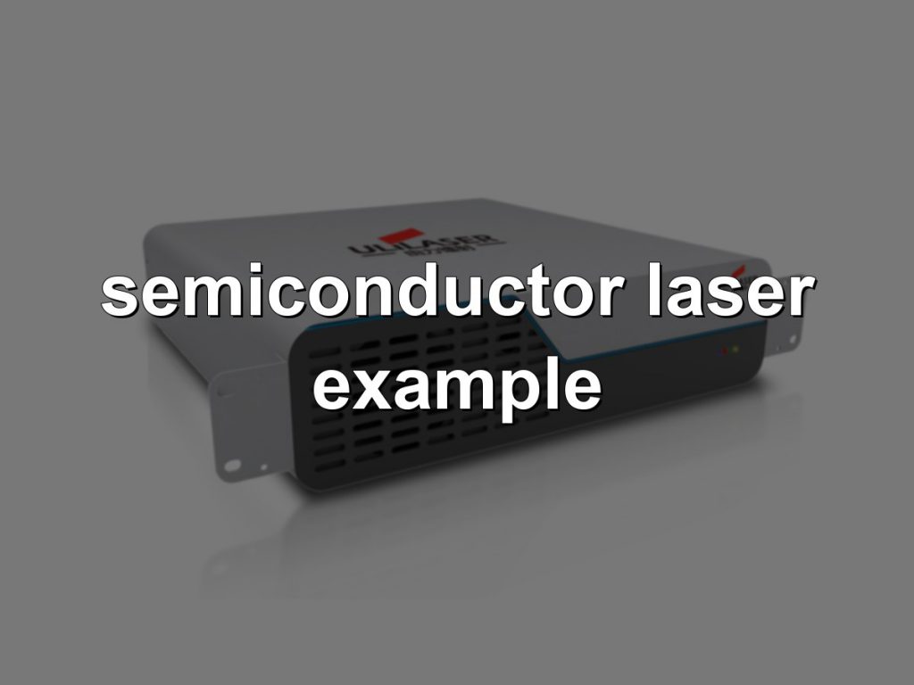
A semiconductor laser example, in a soldering context, is a diode laser module used purely as the heat source: for instance a fiber-coupled 976 nm diode array rated 60 W and focused to a 1.2 mm spot, reflowing SAC305 sol…
A semiconductor laser example, in a soldering context, is a diode laser module used purely as the heat source: for instance a fiber-coupled 976 nm diode array rated 60 W and focused to a 1.2 mm spot, reflowing SAC305 solder paste on a QFN in about 3 seconds. The “semiconductor” in the name refers to the gain medium (a laser diode, not a Yb fiber or a lamp), while the parts being soldered are typically semiconductor packages, connectors or sensor modules. Below are concrete examples of which diode sources are used, what they solder, and how to keep the process in control — laser welding, marking and cutting are outside this scope.

What is a semiconductor laser example in a real soldering station?
A semiconductor laser is a laser diode: current injected across a p–n junction produces stimulated emission at a wavelength set by the material system (GaAs, InGaAs, GaN). In soldering equipment this diode is packaged in one of four ways, and each is a recognisable “example” you will meet on a production floor:
- Single-emitter diode, fiber-coupled (808 / 915 / 976 nm): 10–80 W out of a 105–200 µm fiber, focused to 0.5–2 mm. The workhorse for solder paste and solder ball reflow on small pads.
- Diode bar / array module (915 / 976 nm): 100–500 W, larger spot or line focus, used where a wide seam of joints must be heated simultaneously, e.g. connector pin rows.
- VCSEL array (850 / 940 nm): lower power per emitter, but a rectangular, top-hat intensity profile — useful when you need even heating across a 5 × 5 mm package rather than a Gaussian hot spot.
- Blue GaN diode (450 nm): single-emitter power is modest (3–15 W), but absorptivity in copper at 450 nm is roughly 40–60% versus about 5–10% at 976 nm, which changes the whole energy budget on bare copper pads.
Which wavelength and power fit which soldering job?
Selection starts from absorptivity of the actual top surface, not from the datasheet maximum power. A 976 nm beam couples efficiently into solder (SAC305 absorbs roughly 20–30%) but poorly into bright copper; a 450 nm beam couples well into copper but delivers fewer watts per emitter.
| Diode source | Typical power at work | Spot / line size | Best-fit joints | Watch-outs |
|---|---|---|---|---|
| 808 nm fiber-coupled | 20–50 W | 0.6–1.5 mm | Solder wire on connector pins, TO-can leads | Higher copper reflectance; needs N₂ shield |
| 915 nm fiber-coupled | 30–100 W | 0.8–2 mm | Solder ball reflow, WLCSP, BGA repair | Flux burns if ramp > 150 °C/s |
| 976 nm diode array | 60–300 W | 1–8 mm line | ECU power-module pads, pin headers, shield frames | Thermal cross-talk to adjacent parts |
| VCSEL 940 nm | 5–40 W (array) | 3 × 3 to 10 × 10 mm | Even reflow of small packages, sensor lids | Lower peak irradiance; longer dwell |
| 450 nm GaN | 3–15 W | 0.2–1 mm | Bare copper pads, thin flex, gold-plated pads | Small spot → steep gradients, hot-spot damage |
Three worked examples from electronics manufacturing
1. QFN reflow in an automotive ECU. 976 nm, 60 W, 1.2 mm spot defocused to cover a 4 × 4 mm pad area, scanned at 40 mm/s. Ramp 80–120 °C/s to a 150 °C soak of about 1 s, then to a peak of 245 ± 5 °C held for 2–3 s above liquidus, with N₂ at < 1000 ppm O₂. Closed-loop control reads the pyrometer every 1 ms and cuts diode current, which matters because the diode itself drifts a few percent as it heats.
2. Solder ball attach on a wafer-level chip-scale package. 915 nm, 25 W, 0.8 mm spot, ball-by-ball stepping at 8–12 ms per ball for 0.4 mm pitch. The limiting factor is not power but beam positioning accuracy: ±30 µm placement keeps the beam off the neighbouring ball. This is where CCD vision alignment earns its cost.
3. Connector pin soldering in a sensor module. 808 nm, 40 W with solder wire feeding, 1.5 s per pin. A 1.0 mm spot works for 0.64 mm pins; below that, the beam clips the plastic housing and you get housing melt before the joint wets.
How do I choose a semiconductor laser source for a given joint?
- Start with thermal mass and pad area. Under about 2 mm² of pad, single-emitter fiber-coupled diodes are the practical choice; above about 10 mm², a diode array or VCSEL array heating the whole area evenly beats a scanned small spot.
- Match wavelength to the absorbing surface. Bare copper or gold → shorter wavelength helps; solder paste or solder ball on top → 915–976 nm is efficient.
- Check the neighbours. Measure the temperature rise 2 mm away with a thermocouple; if the adjacent part exceeds its rated reflow exposure, switch to a smaller spot plus scanning, or add a mask.
- Confirm the duty cycle. Diode lifetime and wavelength drift depend on junction temperature — specify water cooling if the duty cycle is above roughly 30% at full power.
- Budget for power verification. A ±5% drift in delivered power is enough to shift peak temperature by 10 °C on a small joint.
What defects appear, and how do I troubleshoot them?
- Cold joint / incomplete wetting: energy delivered below the paste’s needs. Check actual power with a meter, verify the pyrometer emissivity setting, extend the above-liquidus time by 0.5–1 s, and confirm N₂ flow at the nozzle rather than at the regulator.
- Solder spatter and balling: usually ramp rate, moisture or flux outgassing. Drop the ramp to 60–80 °C/s, add a 100–150 °C preheat step, and check paste storage and thaw procedure.
- Pad or package damage, delamination: spot too small for the power, creating a hot spot. Increase spot diameter and reduce power, keeping irradiance constant.
- Excessive voiding under a die or pad: ramp too steep, flux volatiles trapped. Reduce ramp, verify paste deposit thickness, and re-check with X-ray against your void criterion (commonly < 25% for power devices).
- Joint looks dull and oxidised: shield gas problem. Measure O₂ at the work zone; below 1000 ppm is typical, below 500 ppm for fine pitch.
What acceptance checks confirm the process is in control?
- Thermal: peak temperature and time-above-liquidus logged per part, with a Cpk target on peak temperature (e.g. ±5 °C, Cpk ≥ 1.33).
- Visual: fillet shape, wetting angle and no bridging per IPC-A-610 / J-STD-001 criteria.
- X-ray: void percentage and ball/pad alignment on BGA and QFN.
- Mechanical: shear or pull test on a sample basis; cross-section to check intermetallic thickness, typically 1–3 µm for a sound SAC305 joint.
- Source health: daily power check at the nozzle and a monthly beam-profile check; a drifting profile shows up as edge joints failing first.
FAQ
Is a semiconductor laser the same as a diode laser? Yes — both terms describe a laser whose gain medium is a semiconductor junction. In soldering equipment the term usually points to the fiber-coupled diode module that provides the heat.
Can a 976 nm diode laser solder bare copper without flux? Not reliably. Copper absorptivity at 976 nm is only around 5–10% at room temperature, so the first fraction of a second is inefficient; flux or a paste vehicle helps both wetting and coupling. A 450 nm diode reduces that problem but limits available power.
What power do I need for 0.4 mm pitch components? Typically 20–40 W at the work surface with a 0.6–0.8 mm spot; the constraint is beam placement accuracy rather than raw watts.
Why does my diode laser cause spatter on one product and not another? Compare paste lot, stencil aperture and preheat — spatter is nearly always volatiles escaping too fast, not a laser fault.
Does the diode need water cooling? Above roughly 30% duty cycle at full rated power, yes; air-cooled modules are fine for low-duty, low-power work.
If you share your pad size, pitch, paste type and takt time, we can propose a diode source, spot configuration and temperature profile for your specific joint.