


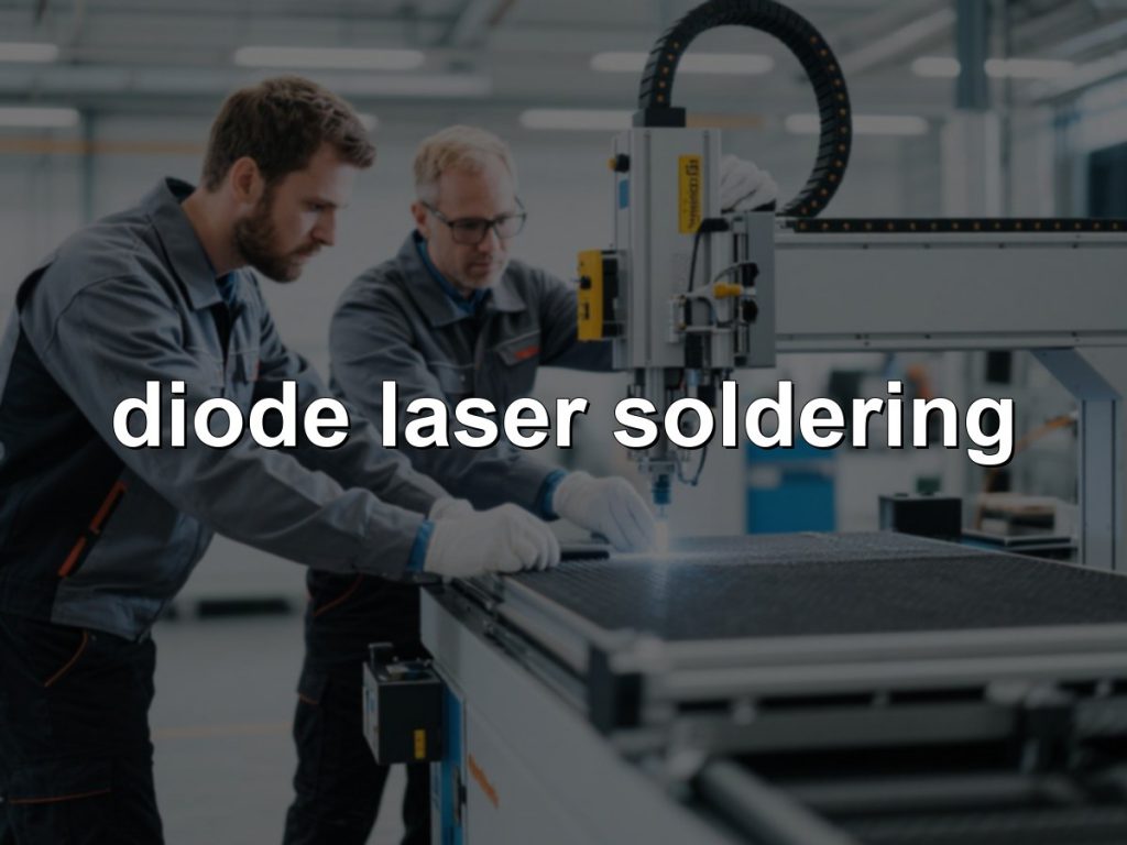
Diode laser soldering is a non-contact reflow process that uses 808–980 nm laser diode energy, focused to a 0.2–1.5 mm spot, to bring a single joint 30–50 °C above the solder liquidus in roughly 100–600 ms while a closed…
Diode laser soldering is a non-contact reflow process that uses 808–980 nm laser diode energy, focused to a 0.2–1.5 mm spot, to bring a single joint 30–50 °C above the solder liquidus in roughly 100–600 ms while a closed-loop pyrometer holds the profile. It is chosen when a soldering iron or hot-air nozzle cannot reach the joint, or when heating the whole assembly would damage neighbouring components — fine-pitch connectors, camera modules, sensor pins, FPC-to-PCB terminations and automotive wire-to-terminal joints. Because the heat is delivered only where the beam lands, board-level thermal load stays low and adjacent low-melting parts are not reflowed.
How does diode laser soldering actually get heat into the joint?
Three things determine whether a diode laser soldering process works: wavelength match, spot definition and temperature feedback.
- Wavelength. 808 nm and 915 nm diodes sit where SnAgCu solder absorbs well; 976 nm modules are used when higher power density is needed in the same footprint. Moving from a 1070 nm fibre source to ~915 nm typically raises absorbed energy in the solder and in the copper pad, so ramp rates are reached at lower delivered power. Copper absorptivity rises sharply as it heats, which is why an open-loop diode laser soldering head can thermally run away on thin pads — closed-loop control is not optional.
- Spot geometry. A flat-top (top-hat) profile heats the whole joint evenly; a Gaussian spot overheats the centre and leaves the toe of the fillet cold. Spot diameter should be 1.2–2× the joint width, aimed with CCD vision so the beam centre sits on the pad–lead interface, not on the component body.
- Closed-loop control. A pyrometer or two-colour sensor sampling at ≥1 kHz drives a PID loop over the diode current. Well-set loops hold peak temperature within ±5 °C joint-to-joint; emissivity is set per surface finish and re-verified whenever the pad finish or solder alloy changes.
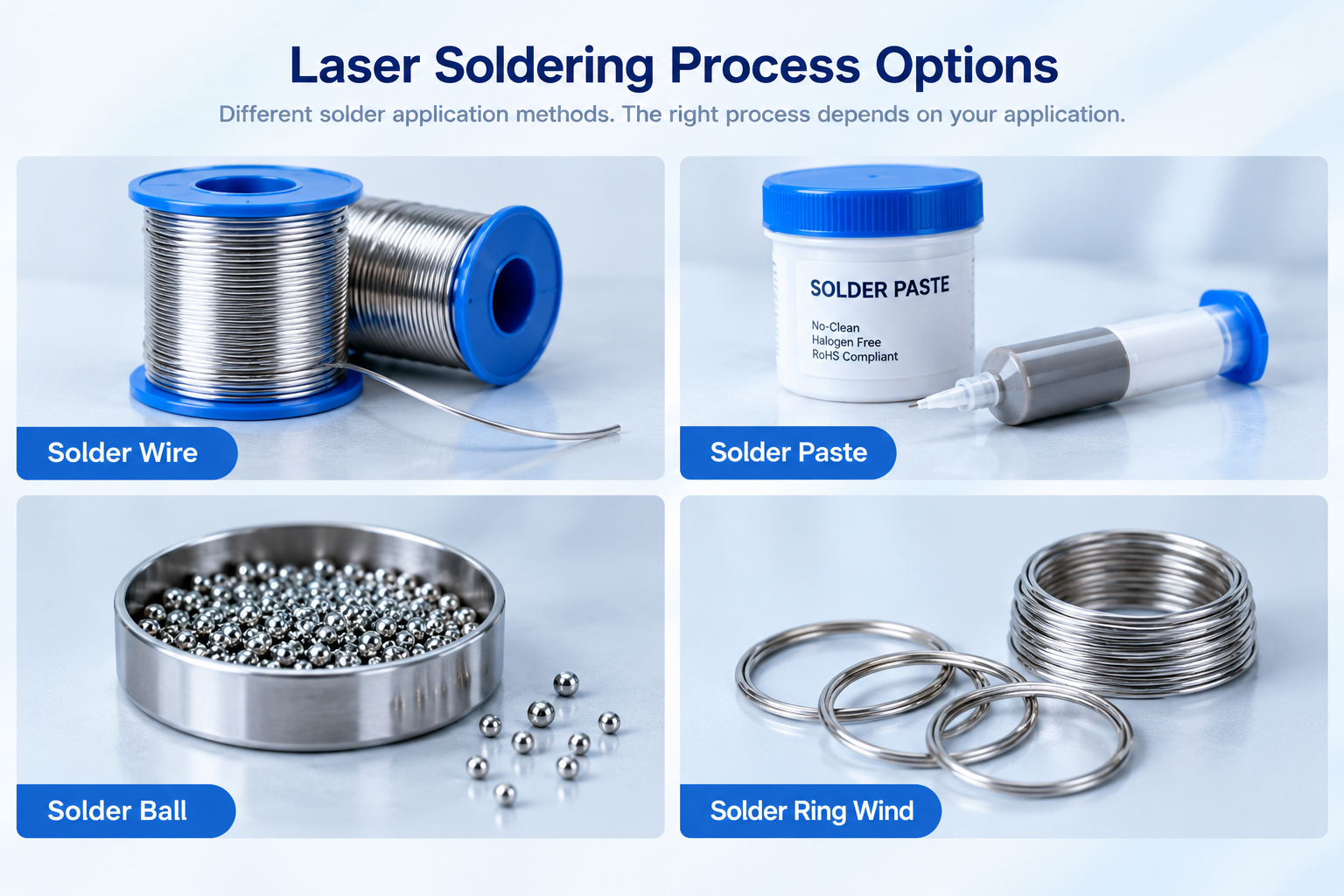
- Feeding. Solder wire (0.3–0.8 mm), solder balls (0.2–0.76 mm) and paste are all used. Feed timing matters — wire entering an already-hot joint flashes and spatters, so feed start should lead the peak by 50–150 ms.
What process window should you start with for diode laser soldering?
Use the table below as a starting point, then tune on your own boards. All values assume SnAgCu alloy, nitrogen shielding at 15–25 L/min, and a fixture holding the part flat.
| Joint type | Solder / feed | Spot Ø | Laser power | Dwell / ramp | Notes |
|---|---|---|---|---|---|
| Connector pin, 0.5–1.0 mm pitch | Wire 0.3–0.5 mm | 0.6–1.0 mm | 30–60 W | 150–400 ms, ramp 100–200 °C/s | Preheat 80–120 °C to protect the housing |
| Solder ball rework, 0.3–0.76 mm | Pre-placed ball + flux | 0.5–0.8 mm | 15–30 W | 80–200 ms | Peak 30–40 °C above liquidus; avoid ball collapse from overshoot |
| Fine-pitch paste joint, 0.3 mm | Type 4/5 paste, 0.1 mm stencil | 0.3–0.5 mm | 10–25 W | Soak 60–90 °C for 1–2 s, then 1–3 s ramp | Soak prevents flux outgassing voids |
| Wire-to-terminal, 0.35–1.0 mm² | Wire 0.6–0.8 mm | 1.0–2.0 mm | 60–100 W | 200–500 ms | Clamp the strand bundle; do not rely on the beam to hold it |
| Ground / shield pad, 3×3 mm and larger | Paste or preform | 2.0–3.0 mm or raster | 100–200 W | 0.5–1.5 s | Raster or dual-head to keep the thermal gradient flat |
Diode laser soldering vs fibre laser, iron and hot air — how do you choose?
| Heat source | Typical spot | Ramp | Board thermal load | Best fit |
|---|---|---|---|---|
| Diode laser (808–976 nm) | 0.2–3 mm, flat-top available | 100–300 °C/s | Very low, localised | Fine-pitch connectors, sensors, wire terminals; high duty-cycle inline cells |
| Fibre laser (~1070 nm) | 0.1–0.5 mm | 200–500 °C/s | Very low | Sub-0.2 mm spots and long working distances; small joints where beam quality dominates |
| Soldering iron | Contact, 0.5–2 mm | Slow, tip-dependent | Conduction into pad | Prototype, rework, large thermal mass with access |
| Hot air / convection | 2–10 mm | 20–60 °C/s | High, whole area | Area array rework; not suitable next to temperature-sensitive parts |
Choose a diode laser soldering head when the joint is small, the ramp must be fast, and there are parts within a few millimetres that cannot see more than 100–120 °C. Choose fibre when the spot must go below 0.2 mm at a long standoff. Diode modules also carry lower running cost than lamp-pumped or fibre sources because electro-optical efficiency is high and there is no consumable to replace on a schedule.
What do diode laser soldering defects look like, and how do you fix them?
- Cold joint, incomplete fillet at the toe. Usually an undersized effective spot rather than low power. Print the beam on burn paper at the working height and measure; then increase dwell by 20 % before raising power. If the pad is heavily oxidised, no amount of energy will wet it — clean or re-flux.
- Solder spatter and balls. Ramp too steep, moisture in the flux, or wire fed into an already-molten pool. Lengthen the preheat segment, dry the parts, and advance wire-feed start by 50–100 ms.
- Charred flux, dark residue. Peak temperature set too high. Bring peak back to 30 °C above liquidus and check that the pyrometer emissivity matches the actual surface; a wrong emissivity is the most common cause of “the profile says 240 °C but the joint looks burnt”.
- Component shift or tombstoning. Asymmetric heating. Re-centre the spot with CCD vision, verify with a joint-level thermal image, and add a light hold-down if the part is under 0.4 g.
- Pad cratering or delamination. Power density too high for the copper thickness. Expand the spot and lower power rather than shortening dwell, and check that the beam is not clipping the board edge or a mask opening.
- Drift across a shift. Lens contamination or diode ageing. Wipe the protective window per shift, log power with an external meter weekly, and re-run a thermocouple-verified profile on a dummy board after any optical change.
What should you check before accepting a diode laser soldering process?
- Recorded profile for every joint type, with peak temperature and time above liquidus inside a defined window, and Cpk ≥1.33 across 30 consecutive joints.
- Fillet appearance to IPC-A-610 Class 2 or 3 as specified: concave fillet, wetting angle under 90°, coverage ≥75 % of the pad–lead interface.
- Cross-section on the first article: intermetallic layer 1–3 µm. Above ~5 µm the joint is brittle and the dwell or peak is too high.
- X-ray voiding on thermal pads ≤25 % area; paste joints checked for head-in-pillow if the paste was printed rather than dispensed.
- Pull or shear test per lot on wire terminals, with the failure mode recorded — wire break is acceptable, joint interface failure is not.
- Post-solder AOI recipe validated against a known-good and a deliberately cold sample, so the inspection actually rejects.
FAQ
Can a diode laser solder through a connector housing? No. The beam must see the joint. What you can do is use a small spot and a short dwell so the housing stays below its softening point, and preheat the assembly to 80–120 °C to shorten the laser-on time.
Is diode laser soldering suitable for high-volume inline production? Yes. With CCD alignment, automatic wire or ball feeding and a fixed optical path, cycle times of 0.3–1.5 s per joint are typical, and the head mounts on standard inline automation modules with SMEMA handshaking.
Why does my pyrometer reading not match the thermocouple? Emissivity mismatch or a spot that is larger than the joint. Set the pyrometer to a spot smaller than the solder pool, calibrate against a thermocouple on a sacrificial board, and re-check after any change in pad finish or solder alloy.
Can I solder lead-free alloys without nitrogen? It is possible on clean, well-metallised pads, but wetting and fillet shape become sensitive to surface condition. Nitrogen at 15–25 L/min is the practical way to hold a repeatable profile at 240–250 °C peak.
Does the diode module need replacement on a schedule? No fixed interval — track delivered power against a reference at the workpiece weekly and replace when it falls outside the window that your profile validation covered.
If you share your joint geometry, alloy and adjacent-component temperature limits, we can map a starting diode laser soldering window for your board and match it to the right head and feeding configuration.