



High-precision laser soldering with visual alignment is a non-contact soldering process in which a machine-vision camera locates the pad, pin, or solder deposit, calculates the X-Y-θ offset, and then directs a focused la…
High-precision laser soldering with visual alignment is a non-contact soldering process in which a machine-vision camera locates the pad, pin, or solder deposit, calculates the X-Y-θ offset, and then directs a focused laser spot onto that exact position while a closed-loop pyrometer holds the joint at a programmed time-temperature profile. “High precision” here is the combination of three things — placement accuracy of the spot (typically ±10 µm or better after calibration), repeatable energy delivery (pulse-to-pulse stability within a few percent), and closed-loop temperature control (commonly ±3–5 °C at the joint). Vision alignment is what makes the first of those possible; it does not, on its own, produce a good joint, which is why the energy and thermal loops must be qualified together with the optics.
What Does “High Precision” Actually Mean in a Vision-Aligned Laser Soldering Cell?
Procurement conversations often stall because “precision” is used loosely. It is worth separating the four specifications that actually govern joint quality, because they are bought and calibrated independently.
- Vision alignment accuracy — how well the camera-derived offset matches the true pad position. Governed by lens resolution, lighting, fiducial quality, and camera-to-laser calibration.
- Spot placement accuracy — where the beam actually lands after the galvo or stage moves. This is the error that shows up as a solder ball sitting half on the pad.
- Spot size and energy density — a 400 µm spot at 30 W and a 1.2 mm spot at 30 W are entirely different processes.
- Thermal repeatability — whether joint top-rated and joint top-rated0,000 see the same profile when the substrate is cold versus heat-soaked.
| Parameter | Common range | What it affects |
|---|---|---|
| Vision alignment repeatability | ±3 to ±10 µm (sub-pixel processing) | Ball/paste placement on fine-pitch pads |
| Camera resolution at object plane | 4–10 µm/pixel, telecentric lens | Fiducial recognition on 0.4 mm pitch and below |
| X-Y compensation range | ±0.3 to ±1.0 mm; θ ±5° | Board and fixture tolerance absorption |
| Laser wavelength | 915 / 976 nm diode; 1070 nm fiber | Absorption in SAC305, copper, and solder mask |
| Laser power (delivered) | 10–150 W, typically well below rated | Ramp rate and time-to-reflow |
| Spot diameter | 0.2–1.5 mm, adjustable | Selective heating and neighbor protection |
| Dwell / pulse time | 50 ms – 2 s | Throughput vs. thermal stress trade-off |
| Closed-loop joint temperature | Setpoint 180–300 °C, control ±3–5 °C | Wetting, IMC growth, component survival |
| Solder ball diameter | 0.15–0.76 mm | Deposited volume per joint |
| N₂ purity / flow | ≥99.99%, 10–30 L/min local | Oxide prevention, fillet formation |
How Does CCD Vision Alignment Work Step by Step?
A production-grade sequence usually looks like this, and each step is a place where an unqualified machine will quietly lose yield:
- Global alignment. Two or more PCB fiducials establish the board coordinate system. Skipping this and relying on fixture datums is the most common cause of “the first board is fine and the tenth is off” complaints.
- Local alignment. The camera images the actual pad, pin, or previously dispensed ball. Telecentric optics and coaxial plus ring illumination are used so the pad edge is not shadowed by solder mask or a connector body.
- Height and focus. A laser displacement or triangulation sensor sets the working distance, because a 20 µm focus error at a 300 µm spot changes the energy density measurably.
- Offset and rotation output. The controller applies X-Y-θ correction to the galvo or motion stage before the beam is enabled — never after, since post-hoc correction means the joint is already partly reflowed.
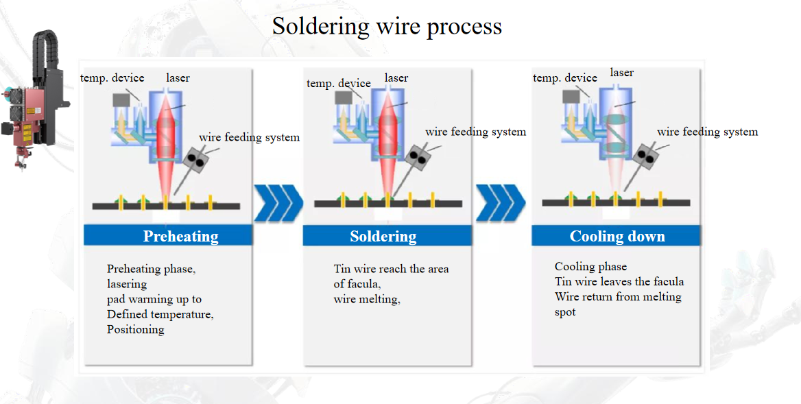
- Energy delivery with feedback. The pyrometer samples the joint and modulates power in real time; a profile is defined by ramp rate, peak, time above liquidus, and cool-down.
- Post-solder inspection. Coaxial AOI checks fillet presence, wetting angle, ball offset, and bridging, and flags joints for rework or X-ray.
Calibration discipline matters more than the camera’s marketing resolution. Camera-to-laser offset drifts with optics warm-up and after any nozzle, lens, or feeder change, so a calibration-target check at the start of each shift — and after every consumable change — is cheap insurance against a drift that only surfaces as a batch of cold joints.
Which Process Parameters Should Be Locked Down Before Production?
Vision alignment tells you where to solder; the profile tells you how. Typical starting windows for SAC305 work:
- Peak joint temperature: 25–40 °C above liquidus (217 °C), i.e. roughly 240–260 °C measured at the joint, not at the laser.
- Time above liquidus: 1–3 s for small joints; longer dwells grow IMC and risk mask scorching.
- Ramp rate: 100–200 °C/s is achievable and desirable for localized heating, but must be balanced against thermal shock in ceramic capacitors and sensors.
- Spot-to-joint ratio: keep the spot 1.0–1.5× the pad width; an oversized spot heats neighboring components and the solder mask between pads.
- Deposit volume: match ball diameter or paste deposit to pad area so the fillet forms without a residual sphere on top.
- N₂ coverage: confirm the shroud actually covers the joint; a misaimed nozzle reads as a wetting problem, not a gas problem.
What Goes Wrong, and How Do You Fix It?
| Symptom | Likely root cause | Action |
|---|---|---|
| Ball sits beside the pad | Camera-to-laser calibration drift, or fiducial misrecognition | Recalibrate with target; verify fiducial contrast and lighting; check panel stretch |
| Cold joint / incomplete wetting | Under-temperature dwell, focus error, oxidized pad | Verify pyrometer reading vs. thermocouple; check working distance; review paste/ball shelf life and pad cleanliness |
| Solder splash and micro-balling | Ramp too fast, moisture or outgassing from paste, spot too small | Lengthen preheat segment; bake boards; widen spot or reduce power density |
| Component shift during reflow | Vision offset applied after beam start, or insufficient hold-down | Confirm offset precedes emission; add vacuum nozzle or local clamp |
| Charred flux, discolored mask | Dwell too long or spot overlapping mask | Shorten time above liquidus; re-size spot; check gas flow isn’t blowing flux away |
| Voids in the joint | Entrapped flux volatiles; poor pad wetting | Adjust profile to let volatiles escape; verify N₂; X-ray to quantify |
| Joint-to-joint variation across the panel | Board warpage changing focus, or thermal crosstalk from adjacent joints | Use height sensing per joint; sequence joints to avoid heat stacking |
How Do You Qualify the Process? Acceptance Checks That Hold Up
Build the qualification around measurable outputs rather than operator judgement:
- Visual: IPC-A-610 Class 2 or 3 criteria for fillet shape, wetting angle, and absence of bridging; document the class in the work instruction.
- Cross-section: IMC thickness typically 1–3 µm; excessive IMC (above ~5 µm) points to over-dwell.
- X-ray: voiding percentage against your internal limit (commonly ≤25% for thermal-critical joints) plus ball offset measurement.
- Mechanical: shear or pull testing on first-article and periodic samples, with a defined minimum based on joint area.
- Repeatability: run 30 consecutive joints and calculate Cpk on joint peak temperature and joint height; Cpk ≥1.33 is a reasonable production gate.
- Alignment audit: measure ball-to-pad offset on a sample under a metrology microscope — this is the only direct proof that the vision loop is doing its job.
When Is Vision-Aligned Laser Soldering the Right Choice?
It earns its cost where heat must be local and placement must be exact: fine-pitch connectors and 0.4 mm-and-below pitch devices, wire-to-pad terminations in automotive sensor and ECU assemblies, optical module and camera module joints adjacent to temperature-sensitive optics, medical device electronics with heat-limited housings, and second-side or rework operations where reflowing the whole board would re-melt existing joints. It is usually the wrong tool for large thermal masses that need bulk heat, or for very high-volume simple joints where reflow is cheaper per joint. Semiconductor packaging applications — die attach, bump repair, and package-level interconnects — are a natural fit because the same vision and thermal loops serve both functions.
FAQ
How accurate is visual alignment compared with mechanical fixturing?
Vision typically achieves ±5–10 µm placement repeatability on a well-lit, high-contrast pad, versus tens of microns for a worn fixture — and it absorbs board tolerance and panel stretch that a fixture cannot. Fixtures still matter for flatness and hold-down; vision replaces the datum, not the support.
Do I need nitrogen for laser soldering?
Not always, but it widens the process window. Local N₂ at 99.99% purity and roughly 10–30 L/min improves wetting and fillet formation, and reduces the dwell needed to reach a good joint, which in turn reduces thermal load on neighbors.
Can it solder 01005 components or 0.4 mm pitch connectors?
Yes, provided the camera resolution at the object plane is around 5 µm/pixel or better, the spot can be reduced to roughly 200 µm, and the deposit volume is matched to the pad. Below that scale, deposit placement accuracy usually limits yield before the laser does.
How do I keep the laser from damaging nearby components?
Three controls: size the spot to the pad, verify the actual joint temperature with a pyrometer rather than trusting laser power settings, and set a hard peak-temperature ceiling. Where neighbors are very heat-sensitive, add a local shield or reduce spot size and extend dwell instead of raising power.
What cycle time should I expect per joint?
For small joints, total time is usually dominated by vision, height sensing, and motion rather than the laser dwell — a realistic planning figure is roughly 0.5–3 s per joint depending on indexing strategy and profile length. Reviewing joint sequencing to avoid thermal crosstalk is often the largest available throughput gain.
If you share your pad geometry, deposit type, and temperature-sensitive neighbors, we can help you map a parameter window and acceptance plan for your specific assembly.