


Laser soldering uses a focused, power-modulated laser beam — most often a 915/976 nm diode laser or a 1070 nm fiber laser — as the heat source to reflow solder ball, solder paste or solder wire at a single joint, with CC…
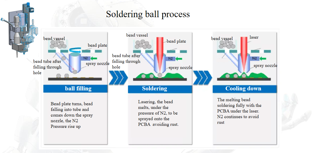
Laser soldering uses a focused, power-modulated laser beam — most often a 915/976 nm diode laser or a 1070 nm fiber laser — as the heat source to reflow solder ball, solder paste or solder wire at a single joint, with CCD vision alignment, closed-loop pyrometer temperature control and post-solder AOI. Its advantages are localized, non-contact heat delivery with fast ramp rates and highly repeatable profiles; its disadvantages are higher capital cost, sensitivity to component tolerances and thermal mass, and throughput limits wherever large areas must be heated.
How does laser soldering actually deliver heat, and why does that matter?
The beam is shaped to a spot of roughly 0.2–2 mm and aimed at the joint — pad, solder and lead/terminal together. Absorbed energy raises the joint at 50–300 °C/s, the solder melts (217–220 °C for SAC305, 183 °C for Sn63Pb37), wets, and solidifies in 0.3–3 s once power ramps down. A pyrometer or two-color sensor samples the joint at 1–10 kHz and closes the loop on power, so the profile is defined in temperature, not in time-at-power.
Because the heat is delivered optically, three things follow that shape every advantage and disadvantage below: no soldering tip touches the work (no contact force, no tip wear, no tip-to-tip variation), the heat-affected zone is small (adjacent parts typically rise 20–60 °C instead of 80–120 °C with an iron), and the process is only as good as the optical access and the part-to-beam alignment.
What are the main advantages of laser soldering?
- Protects heat-sensitive neighbours. Connectors next to electrolytic capacitors, sensors, LEDs and flex tails can be soldered without preheating the whole assembly. Measured temperature rise 2 mm from the joint is commonly 30–50 °C.
- Fast, repeatable ramp with no overshoot. Closed-loop control typically holds peak joint temperature within ±3–5 °C, which matters for IMC growth control and for brittle parts such as ceramic chip caps and crystal units.
- No contact force, no tool wear. Suitable for 0.2 mm-pitch fine-wire joints, thin ribbon and delicate terminals where an iron would bend or scrub the lead. Consumables reduce to the solder feed and shielding gas.
- Handles geometries a tip cannot reach. Recessed connectors, tall housings, and joints shielded from the side are accessible from the top with a small spot.
- Good for high-mix, low-to-mid volume automation. Changing a recipe (power, spot size, ramp, dwell) takes minutes; no fixturing change is needed for a different joint on the same board.
| Characteristic | Laser soldering | Soldering iron (robotic) | Selective hot-air / micro-reflow |
|---|---|---|---|
| Heat delivery | Non-contact, optical | Conduction via tip | Convection + radiation |
| Typical spot / nozzle | 0.2–2 mm | 0.5–3 mm tip | 3–10 mm nozzle |
| Heat-up rate | 50–300 °C/s | 10–40 °C/s | 5–25 °C/s |
| Contact force on part | None | 2–15 N | None |
| Rise 2 mm from joint | ≈30–50 °C | ≈80–120 °C | ≈60–100 °C |
| Joint cycle time | 0.5–3 s | 1–4 s | 20–60 s per board |
| Profile repeatability | Closed-loop, ±3–5 °C | Tip-condition dependent | Nozzle-flow dependent |
What are the disadvantages and where does laser soldering not fit?
- Capital cost per joint is high. A laser source, scanner or galvo, vision, pyrometer, solder feeder and AOI cost more than a robotic iron cell. It pays back on heat-sensitive, fine-pitch or high-value assemblies, not on a simple 2-layer board with 200 large joints.
- Poor at moving heat into thermal mass. Thick ground planes, heavy terminals, press-fit pins and multi-layer power boards with 4 oz copper can sink heat faster than a small spot can supply it. Practical ceiling is roughly 10–15 W of absorbed power per joint; beyond that, preheat or a hybrid approach is needed.
- Line-of-sight and tolerance sensitive. The beam must see the joint. Shadowing from tall components, or part position variation of more than ±0.1 mm, changes the absorbed energy. This is why CCD alignment with fiducial correction is effectively mandatory.
- Process development effort. Absorptivity differs between bare copper, HASL, ENIG, OSP and oxidized pads, and between shiny and matte solder balls. Each new joint family needs a ramp/soak profile validated with cross-sections or pull tests before production.
- Optics maintenance and safety infrastructure. Lens and protective-window contamination degrades power delivery; the cell needs Class 1 interlocked enclosure, and the laser source and chiller add floor space and utilities.
- Verification is indirect. Without AOI or a temperature trace, a cold joint on a hidden barrel is hard to see. Inline AOI plus a sampling pull/shear plan should be budgeted with the machine.
| Parameter | Practical range | Symptom if pushed outside |
|---|---|---|
| Spot diameter | 0.3–2.0 mm | Too small: scorched flux, pinholes; too large: adjacent-part heating |
| Ramp rate | 50–300 °C/s | Too fast: solder spatter, wicking away from pad |
| Peak joint temp (SAC305) | 235–255 °C | Low: cold joint / poor filleting; high: IMC thickening, pad lift |
| Time above liquidus | 0.3–1.5 s | Long: dull, grainy fillet, flux burn-off |
| N₂ shielding (O₂) | <1000 ppm | Higher: oxidation, dewetting on OSP copper |
How do you decide whether laser soldering is the right process for a joint?
Run three checks before quoting equipment. First, thermal mass: if the joint sits on a plane larger than about 100 mm² of 2 oz copper, expect to need preheat or to reject the application. Second, access: confirm a straight, unobstructed cone from above at 15–25° off-axis, and that component position repeats within ±0.1 mm. Third, value: laser soldering is usually justified where the assembly cost of a thermal failure (sensor drift, connector rework, delamination) exceeds the per-joint premium, or where a 0.2–0.4 mm pitch joint simply cannot be reached by a tip.
For a mixed board, the common answer is hybrid: laser for the heat-sensitive and fine-pitch joints, selective hot-air for the large connectors, both on one inline platform.
Which defects appear in production, and how are they corrected?
| Symptom | Likely cause | Corrective action |
|---|---|---|
| Cold joint, dull non-wetting fillet | Under-power, dirty optics/window, oxidized pad | Verify delivered power with an external meter, clean window, extend soak 0.2 s, check pad finish |
| Solder balling / spatter | Ramp too fast, flux outgassing, wet ball | Reduce ramp to 80–120 °C/s, dry/reflow ball feed, check N₂ flow |
| Scorched flux, dark residue | Spot too small for the joint, excessive peak temp | Increase spot 0.1–0.2 mm, cap peak at 250 °C, shorten time above liquidus |
| Wicking or solder drawn up the lead | Lead hotter than pad; beam offset toward the lead | Re-center beam on pad edge, verify CCD offset, slow the ramp |
| Intermittent cold joint on same joint every cycle | Thermal-mass variation or pyrometer mis-sighting | Confirm emissivity/spot on the joint, not the component body; add thermal-mass compensation to the recipe |
FAQ
Is laser soldering faster than a soldering iron? For a single small joint, yes — 0.5–3 s per joint versus 1–4 s — but the real gain is in ramp control and reduced rework, not cycle time. On a board with hundreds of large joints, selective reflow is usually faster overall.
Can laser soldering replace reflow for a whole board? No. It is a selective, point-to-point process. Reflow remains the economical choice for high joint counts; laser soldering serves heat-sensitive, fine-pitch or rework joints.
Does it work with solder wire, paste and preforms? Yes. Wire (0.3–0.8 mm) is common for connectors, solder balls 0.2–1.0 mm for small pads, and paste is dispensed where a preform fits better. Feed accuracy of ±0.05 mm keeps deposit volume consistent.
How much maintenance does the optical path need? Inspect the protective window and lens weekly under a scope, clean with optics-grade solvent, and verify power monthly. Contamination shows up first as a slow rise in required power and later as cold joints.
Do I need AOI with laser soldering? Not strictly, but because the joint cools in milliseconds and little visual evidence remains, inline AOI is the practical way to catch cold joints and missing solder before functional test.
If you have sample boards with connector or sensor joints you are unsure about, send them over and we will run a profile trial and report the achievable ramp, peak temperature and pull strength for each joint.