



Laser soldering in consumer electronics manufacturing is a selective, non-contact joining process in which a focused diode or fiber laser delivers a controlled energy pulse to a specific pad-and-solder combination, while…
Laser soldering in consumer electronics manufacturing is a selective, non-contact joining process in which a focused diode or fiber laser delivers a controlled energy pulse to a specific pad-and-solder combination, while a closed-loop pyrometer holds the joint at a defined temperature profile. It is used where reflow, hot-bar or iron soldering cannot meet the combined constraints of fine pitch, thin flex substrates, heat-sensitive plastic housings and short cycle time — typically FPC connectors, camera modules, USB-C shells, shield-can grounding tabs and 0201/01005 passives. This article covers where the process fits, which parameters to specify, how failures present, and what acceptance checks to run.
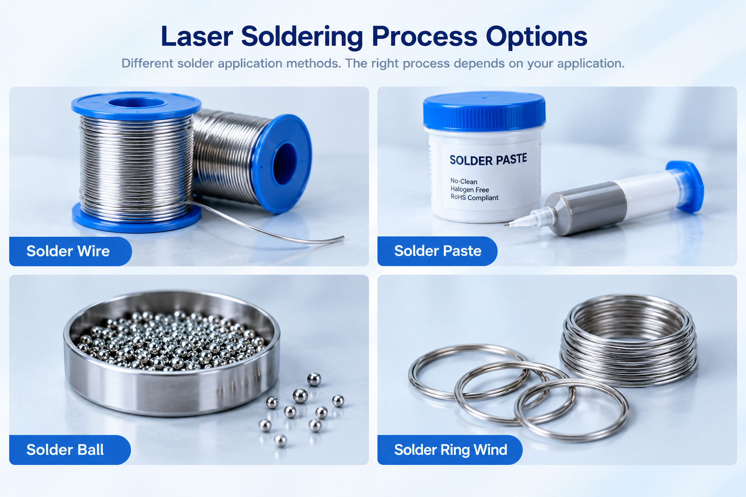
Where does laser soldering fit in consumer electronics assembly?
The decision rule is straightforward: if the joint is small, sits next to a polymer part or a battery, or sits on a substrate that warps under whole-board heating, a local heat source is the lower-risk option. Typical insertion points:
- FPC-to-PCB and FPC-to-connector joints. 0.3 mm pitch flex tails on polyimide, where the surrounding coverlay and stiffener cannot take a second reflow excursion.
- Camera module and VCM flex bonding. Lens holders and actuators are already assembled and temperature-sensitive when the flex is joined.
- USB Type-C and board-to-board connector shells. LCP/PA9T housings deform above roughly 260–280 °C, so energy must be confined to the shell tab.
- Shield-can and shield-frame grounding tabs. Often reworked or added after the main reflow, with the populated board alongside.
- 0201/01005 passives and antenna/EMI modules on HDI and rigid-flex, where paste volume is below what a stencil can reliably deposit.
- TWS earbud boards, battery protection boards and miniature speaker/mic wire-to-pad joints — wire feeding with a 0.2–0.4 mm solder wire.
It is not a whole-board replacement for reflow. Throughput economics favour laser for selective joints, rework, and boards with mixed thermal constraints.
Which laser source, spot size and energy window should you specify?
Two heat sources dominate: 980 nm diode lasers (good absorption in solder and copper, lower cost, 10–80 W) and 1070 nm single-mode fiber lasers (tighter spot, higher power density, 50–150 W) for larger tabs. Beam delivery is galvo-scanned or a fixed head over an XY table; both are usually paired with a coaxial CCD and a height sensor for focal-position compensation on warped flex.
| Joint type | Laser / power | Spot diameter | Dwell / energy | Solder feed | Notes |
|---|---|---|---|---|---|
| 0201 / 01005 passive | Diode, 8–20 W | 0.3–0.5 mm | 150–400 ms | Paste dot 0.10–0.15 mm, or 0.20 mm ball | Preheat 100–130 °C to limit tombstoning |
| 0.3 mm pitch FPC connector | Diode, 5–15 W | 0.2–0.3 mm | 200–500 ms | Paste dot or 0.2 mm ball | Nitrogen assists; keep adjacent coverlay <200 °C |
| Camera module flex | Diode, 10–20 W | 0.4 mm | 150–300 ms | 0.2–0.3 mm ball | Fixture must constrain flex flatness |
| USB-C shell tab | Fiber, 60–120 W | 1.5–3.0 mm | 0.4–1.2 s | 0.5–0.8 mm wire | Shield gas to protect housing; ramp in 2 steps |
| Shield-can grounding tab | Fiber, 30–60 W | 0.8–1.5 mm | 0.3–0.8 s | 0.5 mm wire | Verify tin-plated tab thickness; nickel needs more energy |
Independent of the table, hold these process windows: peak joint temperature 235–260 °C for SAC305 (liquidus 217–220 °C), 0.5–2 s above liquidus, ramp 150–300 °C/s, and a measured peak below 300 °C at the pad to stay clear of polyimide blistering and pad cratering. Confirm the pyrometer spot actually covers the joint, not the surrounding laminate — emissivity mismatch is the single most common cause of a “correct” setpoint producing a cold joint.
What do common defects look like and how do you fix them?
Most laser soldering failures trace back to energy delivery, solder volume, or atmosphere — in that order. Work through the table before changing the alloy or the flux.
| Symptom | Likely cause | Corrective action |
|---|---|---|
| Solder micro-balls / spatter around the joint | Flux outgassing driven too fast; paste too thick or expired | Add a 50–100 ms low-power pre-step, lower the ramp, reduce paste dot 10–20%, verify paste thaw time and shelf life |
| Dull, grainy fillet; incomplete wetting | Energy shortfall, oxidized pad, focus drift | Raise energy 10–20%, re-check focal spot on a test card, add N₂ to <1000 ppm O₂, verify pad finish and contamination |
| Pad crater, flex burn-through, epoxy smell | Peak temperature too high or spot too small for the pad | Defocus to widen the spot, cap peak at 300 °C, lengthen dwell instead of raising power |
| 0201 tombstoning | Asymmetric heating or uneven paste deposit | Centre the spot on the pad pair, check dispense symmetry, reduce ramp rate |
| Voids above 25% on X-ray | Trapped flux volatiles; short time above liquidus | Extend dwell 100–200 ms, lower flux solids, add a short soak near 200 °C |
| Connector housing softening or whitening | Stray beam energy on the polymer body | Reduce spot or use beam shaping, add a gas shield, re-aim to the tab only |
| Bridging on fine pitch | Solder volume too high | Step down ball diameter (0.25 → 0.20 mm) or paste dot volume by 15% |
If results drift across a shift with no parameter change, inspect the protective window and nozzle for flux condensate first, then re-verify focus and pyrometer calibration. A dirty window typically costs 10–15% of delivered energy before any alarm appears.
Which acceptance checks qualify the process?
- Visual (IPC-A-610 Class 2/3): concave fillet, wetting angle ≤30° on the pad, solder wetted to the component termination, no spatter above 0.1 mm inside defined keep-out zones.
- X-ray: voiding ≤25% of joint area for bottom-terminated and connector joints; check for open joints under shell tabs.
- Cross-section (first article and change control): intermetallic layer 1–4 µm, no Kirkendall voids, no lifted pad or laminate separation.
- Mechanical: shear test on chip components — typical internal limits are ≥5 N for 0402 and ≥2 N for 0201; pull test on wire joints per your internal spec.
- Thermal verification: thermocouple on the nearest heat-sensitive component must stay below its rated limit (commonly <150 °C for battery-adjacent parts, <250 °C at connector housings) during the pulse.
- Repeatability: peak-temperature Cpk ≥1.33 across a 30-board run before releasing to production; daily focus-spot check, weekly power-meter check, and pyrometer re-calibration against a thermocouple on a dummy board.
FAQ
Can laser soldering replace reflow for an entire board?
No. It is a point-by-point selective process suited to heat-sensitive, fine-pitch or rework joints. Boards with hundreds of joints are better served by reflow, with laser reserved for the joints reflow cannot reach safely.
Does the laser damage components next to the joint?
With a correctly sized spot and a 0.2–1.0 s pulse, the thermal field typically falls off within 1–3 mm, and adjacent component temperature rises are usually held below 40–60 °C. Verify with a thermocouple on your actual board rather than relying on a rule of thumb — thin flex and copper-pour density change the result substantially.
Is nitrogen mandatory?
Not mandatory, but recommended for lead-free no-clean assemblies. Holding oxygen below 1000 ppm measurably improves wetting on OSP and immersion-silver pads and reduces micro-ball formation on fine pitch.
What cycle time should I budget?
Plan 0.2–1.0 s of laser time per joint plus 0.3–0.8 s for vision alignment and moves. Galvo scanning with a split beam or dual heads is the usual way to keep a multi-joint connector under a few seconds per unit.
Can it solder wire and through-hole parts?
Wire feeding with 0.2–0.8 mm solder wire is standard for connector shells and grounding tabs. Through-hole is possible but limited by barrel depth — the beam heats the top surface, so deep barrels need a different approach.
If you share your joint geometry, substrate stack-up and adjacent-component temperature limits, we can map a parameter window and fixture concept for your specific assembly.