


Laser soldering for flexible PCB assembly uses a focused, closed-loop-controlled laser spot to reflow one joint at a time in roughly 0.3–1.5 seconds, so the polyimide substrate, coverlay adhesive and neighbouring low-tem…
Laser soldering for flexible PCB assembly uses a focused, closed-loop-controlled laser spot to reflow one joint at a time in roughly 0.3–1.5 seconds, so the polyimide substrate, coverlay adhesive and neighbouring low-temperature parts never see the full 245–260 °C panel excursion of a reflow oven. It is a selective process: you still reflow the bulk of the board conventionally and use the laser where thin flex, heat-sensitive components, odd-form connectors or stiffener steps make oven reflow risky. The result is a joint whose peak temperature and time-above-liquidus are measured and logged per joint, which is what makes the process auditable for automotive and medical flex assemblies.
Why does laser soldering suit flex circuits better than oven reflow?
On a 25–50 µm polyimide flex with a 12–35 µm copper layer, the failure modes of oven reflow are mostly thermal-history problems rather than solder problems: coverlay blistering, adhesive delamination, panel warp, connector body creep and discoloration around stiffener boundaries. A laser delivers energy only where the joint needs it, and a pyrometer or two-colour sensor closes the loop on the actual joint temperature rather than the oven air temperature.
| Factor | Convection reflow of a flex panel | Selective laser soldering |
|---|---|---|
| Substrate thermal exposure | Whole panel at 245–260 °C for 40–90 s | Joint area only; bulk panel typically stays below 120–150 °C |
| Coverlay / adhesive risk | Blistering and delamination accumulate over panels | Adjacent zone affected within roughly 1–3 mm; controllable by spot size |
| Thin-panel warp | Needs carrier or pallet; warp still common | Low bulk heating, but vacuum fixturing is still mandatory |
| Mixed-temperature assemblies | Limited by the lowest-rated component on the panel | Can solder beside 150 °C-rated parts and HT plastic connectors |
| 3D / stepped / stiffened regions | Shadowing and uneven heat transfer | Direct line-of-sight to the joint; no shadowing |
| Traceability | Oven profile per product | Per-joint temperature curve, stored by serial number |
| Throughput model | Batch | 0.3–1.5 s per joint plus motion; galvo systems reach several joints per second |
The trade-off is that laser soldering is a serial process and depends entirely on joint access. Design reviews should confirm line-of-sight to every joint, a stable backside support under each pad, and a coverlay opening that exposes the full land plus 0.1 mm.
Which parameters work for polyimide flex circuits?
The dominant control variable is not laser power but the temperature profile at the joint. Diode sources at 808–980 nm are the common choice because the power density is easy to shape with a zoom spot and the energy couples predictably into copper and eutectic or SAC alloy; shorter wavelengths couple more strongly into copper, which helps on thin traces but punishes you if the spot clips a ground plane.
| Parameter | Typical range | Practical note |
|---|---|---|
| Spot diameter at work plane | 0.6–3.0 mm | Roughly 1.2× the land so the fillet, not the coverlay, absorbs the energy |
| Laser power | 10–60 W | Higher on joints tied to a power/ground plane |
| Ramp rate | 50–200 °C/s | Fast ramp reduces adhesive soak time but raises overshoot risk |
| Peak joint temperature (SAC305) | 230–245 °C | Melting 217–220 °C; keep peak margin small on flex |
| Time above liquidus | 0.5–2.0 s | Longer TAL grows IMC and stresses the pad-to-PI bond |
| Fixture preheat | 80–120 °C | Reduces required laser power and thermal shock on thick ground planes |
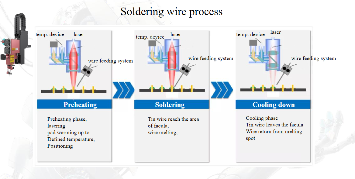
| Solder feed | Ball 0.2–0.76 mm; wire 0.3–0.5 mm; paste dot 0.25–0.5 mm | Ball feeding gives the most repeatable volume at fine pitch |
| Nitrogen shield | 99.99 %, 15–25 L/min local | Improves wetting on ENIG and immersion tin, which flex usually uses |
| Placement accuracy | ±15 µm | CCD with local fiducials, not panel-level only |
Two things trip people up on first articles. First, pyrometer emissivity: an uncalibrated sensor can read 20–30 °C low on a shiny ENIG land, so always validate with a fine-wire thermocouple bonded next to the joint. Second, copper asymmetry — the same joint on a flex tail with 18 µm copper and on a stiffened section with a 70 µm copper plane needs different power, even though the pad geometry looks identical.
How do you fixture and align flexible circuits for laser soldering?
- Support directly under the pad. A vacuum chuck with pockets that put a hard stop within 0.1 mm below the joint prevents the flex from flexing under galvo motion or wire-feed contact. Unsupported joints show variable peaks of ±15 °C.
- Local fiducials, two per part. Polyimide stretches during lamination and coverlay cure; panel-level fiducials alone can leave 100–200 ppm of residual error across a 250 mm panel. Local alignment plus per-part distortion compensation keeps placement inside ±15 µm.
- Clamp within 3–5 mm of the joint. Kapton tape is not a fixture — it creeps at preheat temperature. Use vacuum or mechanical fingers.
- Design for anchor. Capture pads, teardrops and a coverlay opening 0.1 mm larger than the land reduce pad lift and solder wicking under the coverlay.
- Keep the spot off the coverlay edge. Adhesive bond lines are the weakest thermal link; a 0.2 mm overlap repeated over thousands of joints is enough to start a blister.
What defects appear, and how do you troubleshoot them?
| Symptom | Likely cause | Action |
|---|---|---|
| Pad delamination or coverlay blister | Peak temperature or TAL too high; spot overlapping adhesive | Drop peak to 235 °C, cut TAL below 1.5 s, shrink spot, verify with thermocouple |
| Ball not collapsing / cold joint | Energy sunk into plane, misalignment, low N2, oxidised pads | Raise power or add preheat, re-run CCD alignment, check flow, confirm finish date code |
| Solder wicked under coverlay, short | Over-feed, excessive TAL, tight coverlay opening | Reduce ball size one step, shorten TAL, widen coverlay opening to land + 0.1 mm |
| Browning around the joint | Sensor misreading (emissivity), overshoot on thin copper | Recalibrate pyrometer, reduce ramp, add a short hold before peak |
| Component shift or tombstone | Uneven pad heating, ramp too fast for the paste flux to activate | Balance spot position across both lands, slow ramp to 80–100 °C/s |
| Joint crack after thermal cycling | Excess IMC from long TAL; CTE mismatch at the flex transition | Cap TAL at 2 s, inspect cross-section for IMC over 4 µm, add stress relief in the land design |
How do you qualify and inspect the process?
- First article: thermocouple on the joint, record peak temperature, TAL and ramp for the highest- and lowest-mass joints on the panel. Release only when both sit inside the window.
- Visual: assess fillet, wetting angle and pad coverage against IPC-A-610 flex criteria and J-STD-001; check for discoloration at the coverlay boundary.
- Cross-section: confirm IMC thickness in the 1–4 µm band and check for pad-to-polyimide separation; dye-and-pry on a sample per lot.
- Mechanical: 90° peel or pull on a test coupon built into the panel border, with a defined minimum force per joint type.
- Reliability: thermal cycling −40 to +125 °C for 500–1000 cycles with in-situ resistance monitoring, plus damp heat where the flex carries conformal coating.
- In-line: AOI after soldering for fillet shape, offset, bridging and missing ball; SPC on peak temperature and joint height, not just pass/fail.
FAQ
Can laser soldering replace reflow entirely on flex assemblies? Not usually. Most production lines reflow the high-density area conventionally and use laser soldering for the joints that reflow cannot reach safely — connectors, stiffened sections, flex-to-rigid transitions and heat-sensitive parts. The decision is made per joint, not per panel.
Will the laser damage the polyimide? Polyimide itself withstands well above soldering temperatures; the practical limits are the coverlay adhesive, the bond between pad and substrate, and any temperature-sensitive component nearby. Keeping the spot inside the land and the peak near 235 °C for under 2 seconds keeps the bulk substrate cool.
Do I need nitrogen? It is strongly recommended on ENIG and immersion tin, which are the usual flex finishes. Without a local shield, wetting angle degrades and cold joints appear on joints that look thermally correct on the profile.
What throughput should I expect? With a galvo head, 0.3–1.5 s of lasing per joint plus a few tens of milliseconds of move time; a scanner-based cell typically handles several joints per second on adjacent pads, while ball feeding and vision add the rest of the cycle.
Can the same cell handle solder ball, paste and wire? Yes — multi-feed heads switch tooling per program, which matters when a flex assembly mixes a 0.3 mm ball joint at fine pitch with a wire-fed connector tab on the same panel.
If you share your flex stack-up, pad pitch and joint count per panel, we can propose a laser soldering configuration and run first-article profiles with you.