


Choosing laser soldering equipment for semiconductor package interconnects comes down to matching five specifications to your actual package: the allowed thermal budget, the solder delivery format, the vision and inspect…
Choosing laser soldering equipment for semiconductor package interconnects comes down to matching five specifications to your actual package: the allowed thermal budget, the solder delivery format, the vision and inspection resolution, the closed-loop temperature control performance, and the inline automation interface. Get those five right and the machine will hold a repeatable profile at fine pitch with a narrow peak-temperature spread; get any one wrong and you will spend the first months of production reworking cold joints, chasing package warpage, or rejecting units at AOI. The sections below walk through each decision with the numbers to ask vendors for during evaluation.
What thermal budget does your package actually allow?
Semiconductor packages are usually limited by the substrate and mold compound, not by the solder. FR-4 substrates soften around 150–180 °C, BT around 180–200 °C, and many mold compounds and die-attach adhesives have their own ceilings. Because a laser delivers energy only where the beam lands, the joint can reach 235–245 °C while the substrate 3–5 mm away stays below 120 °C — but only if the beam spot, dwell time and power are tuned together. Ask for a measured profile on a daisy-chain coupon, not a datasheet curve.
| Parameter | Typical laser-soldering window | How to verify before purchase |
|---|---|---|
| Peak joint temperature | 230–250 °C for SAC305 (217 °C liquidus + 15–30 °C) | Thermocouple profile on a daisy-chain coupon, 30 consecutive joints |
| Ramp rate | 50–200 °C/s | Controller log; above ~200 °C/s expect spatter and die stress |
| Time above liquidus | 0.3–1.5 s (vs 45–90 s in reflow) | Profile export; shorter TAL limits IMC growth |
| Package body ΔT | Keep joint-to-body gradient under 30–40 °C | IR camera or 3+ thermocouples across the package |
| Beam spot diameter | 0.3–3 mm; roughly 1.0–1.5× the joint footprint | Beam profiler at the working plane, not at the source |
| Substrate temperature | Below Tg, measured 3–5 mm from the joint | Thermocouple on the substrate surface during the cycle |
Which solder delivery format matches your interconnect?
This decision is driven by pad geometry and required volume control, and it usually narrows the machine shortlist faster than any other criterion. A system that feeds balls cannot print a 0.2 mm pitch pad array, and a paste dispenser is a poor match for a 0.6 mm connector terminal that needs a fillet.
- Solder ball. Best for BGA, WLCSP, Cu pillar and PoP interconnects, 0.15–0.76 mm. Check ball placement repeatability (±25 µm is a reasonable ask), the fluxing method (dip, spray or stamp), and whether the head can be changed without re-teaching.
- Solder paste. Best for fine-pitch pads, 0.2–0.4 mm pitch arrays and connector footprints. Ask for dispense-volume repeatability (±5% within a run), minimum deposit diameter, and how the system handles paste viscosity drift over a shift.
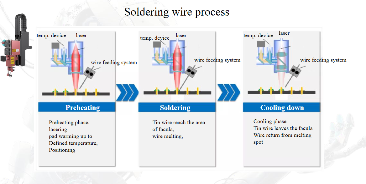
- Solder wire. Best for through-hole pins, lead-frame terminals and wire-to-pad joints, 0.2–0.8 mm. Confirm wire-feed resolution (±0.1 mm), feed angle adjustment, and whether flux-cored wire is supported without clogging the nozzle.
If your product mix spans more than one of these, confirm the platform is genuinely modular — a shared motion and vision stage with swappable feed heads — rather than three separate machines with separate recipes.
How much vision alignment and AOI resolution do you actually need?
Placement accuracy should be specified relative to your smallest pad, not as a headline number. For 0.4 mm pitch, ±25 µm placement is usually adequate; at 0.2 mm pitch, target ±10–15 µm with a telecentric lens and fiducial-based correction. Cameras in the 2–5 MP range with a field of view matched to the package are typical, and you should confirm the pixel resolution at the working plane in µm/px — not the sensor’s total pixel count. Warped substrates are common in thin packages, so a height map or laser profilometer that corrects focus and Z-height per unit is worth more than extra megapixels.
For post-solder AOI, 5–10 µm/px is sufficient to judge fillet shape, wetting angle, bridging, ball offset and void area. Decide early whether inspection runs inline (adds cycle time but catches drift within a shift) or offline, and require the AOI recipe to be exportable so you can audit it against IPC-A-610 Class 3 criteria and IPC-7095 voiding limits.
How do you validate closed-loop temperature control before buying?
Closed-loop control is the difference between a lab tool and a production tool. The loop should read joint temperature from a pyrometer sampling at 1 kHz or faster, with a measurement spot no larger than the joint, and modulate laser power in real time rather than running a fixed open-loop pulse. During a demo, ask for these checks:
- Run 30–50 joints and calculate the peak-temperature spread; ±5 °C is a realistic target, with overshoot under 10 °C.
- Verify emissivity calibration against a thermocouple on the same coupon — an uncalibrated pyrometer can read 20–30 °C low on shiny solder.
- Confirm the recipe is transferable: save it, restart the machine, and check the profile repeats.
- Ask how the system compensates for substrate thermal mass differences between a 0.4 mm and a 1.6 mm board.
Common symptoms and where to look: cold joints or incomplete fillets usually mean low peak temperature or a beam spot offset from the pad; spatter points to ramp rate above ~200 °C/s or moisture in the paste; voids and flux entrapment usually trace back to insufficient preheat or a profile with no soft ramp below 150 °C; pad cratering and die cracks indicate too much energy delivered too fast and should be checked with a cross-section on the first-article units.
What does inline integration and throughput look like?
Compute throughput from the cycle, not from a brochure figure: heating time (0.3–1.5 s) plus move and settle time (0.2–0.5 s) per joint gives roughly 600–1,500 joints per hour per head, and multi-head or dual-lane configurations scale from there. Confirm the machine speaks SMEMA at the load and unload ends, supports the MES or SECS/GEM interface your factory uses, and stores recipes with revision control. Also ask about utilities and consumables — nitrogen demand, chiller or air-cooling, laser diode lifetime and replacement cost — because these dominate cost of ownership far more than purchase price.
For first-article acceptance, plan a short qualification: 30 joints for profile capability, a cross-section for IMC thickness and fillet geometry, ball shear or pull testing per JESD22-B117, void measurement against IPC-7095, and a 4-hour run to confirm the recipe does not drift. Note that this is soldering with a laser heat source and a solder alloy — not laser welding, which fuses base metal without filler and sits outside our scope.
FAQ
Can laser soldering equipment handle 0.2 mm pitch and below?
Yes, with paste jetting and a beam spot in the 50–150 µm range. The practical limits are flux residue removal and bridging risk between adjacent deposits, so qualification should include a bridging check across at least 200 joints.
What throughput should I expect in production?
For single-point soldering, 600–1,500 joints per hour per head is a realistic working range depending on joint size and profile length. Multi-head gantries or dual-lane platforms are the usual route above that.
Do I need nitrogen?
For SAC305 on clean OSP or ENIG pads with an active no-clean flux, wetting is often acceptable without it. If you are soldering bare copper, thick OSP, or larger thermal masses, use 99.99% N₂ and hold oxygen below 1,000 ppm — below 100 ppm for the most oxidation-sensitive joints.
Why are my joints spattering?
Check ramp rate first (reduce below 150 °C/s), then paste condition and storage — moisture pickup after a shift at room temperature is a frequent cause. If spatter persists, inspect nozzle alignment and confirm the beam spot is not striking the flux deposit before the solder.
How is this different from laser welding?
Laser soldering melts a filler alloy that wets and bonds to pads at 230–250 °C, with flux and inspection criteria from IPC standards. Laser welding fuses the base metals themselves; it is a different process with different equipment and is not part of our product range.
If you send us your package cross-section, pad pitch and target profile, we can recommend a configuration and run a sample coupon so you can compare measured results against your acceptance criteria.