


Solder bridging in fine-pitch laser soldering almost always traces back to one of three things: too much solder on the pad, heat delivered faster than the flux can vent, or a beam/placement offset that lets molten solder…
Solder bridging in fine-pitch laser soldering almost always traces back to one of three things: too much solder on the pad, heat delivered faster than the flux can vent, or a beam/placement offset that lets molten solder reach a neighbouring pad. Because a laser delivers energy in a spot rather than through a whole-board oven, the process window is narrower and the failure is more repeatable — which is good news, because it means you can find and close it with a few controlled adjustments. The sequence that works: fix deposit volume first, then the heating profile, then beam-to-camera alignment, then verify with AOI and a first-article cross-section.
What actually causes bridging between fine-pitch pads?
In a reflow oven, bridging is mostly a stencil-print problem. Under a laser, four mechanisms dominate, and they look different under the microscope — which is how you tell them apart:
- Excess solder volume. A 0.4 mm pitch joint needs roughly 60–80% of the solder that a 0.5 mm pitch pad takes. Oversized solder balls, worn stencil apertures or a paste deposit that has slumped after long idle time all push volume past what the pad gap can hold.
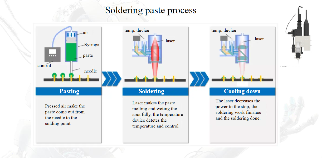
- Flux volatiles venting explosively. Laser ramp rates of 60–150 °C/s bring the paste to liquidus before solvent fully escapes. The escaping gas ejects micro-spheres of solder that land on the solder mask sliver and form a bridge on the next reflow pass, or immediately.
- Beam or deposit offset. If the laser spot overlaps the neighbouring pad, or the ball-placing nozzle is 50 µm off, the adjacent deposit melts and the two liquids coalesce. This is the most common cause of bridges that appear only on one side of a connector or only at one end of a row.
- Pad and mask geometry. A solder mask sliver narrower than about 50 µm, mask thickness variation, or a copper-defined pad with no mask dam gives molten solder a continuous path between conductors regardless of how good the laser profile is.
Which parameters should you tighten first, and to what values?
The table below is a practical starting window for 0.4 mm pitch and finer, SAC305 solder, on an inline laser soldering cell with CCD alignment and closed-loop temperature control. Treat it as a starting point to be validated on your own boards, not as a fixed recipe.
| Parameter | Starting range for fine pitch | Effect on bridging | How to verify |
|---|---|---|---|
| Solder ball diameter / paste deposit | Ball 0.6–0.8× pad width (e.g. 0.20–0.25 mm ball at 0.4 mm pitch); paste area ratio ≥0.66, stencil 0.08–0.10 mm, Type 6 powder (5–15 µm) | Primary driver — excess volume has nowhere to go but across the gap | 3D SPI on paste; weigh or measure 10 deposits; ball diameter incoming inspection |
| Laser spot diameter at the work plane | 1.2–1.8× pad width, spot edge kept ≥0.05 mm inside the pad boundary | Spot spill onto the neighbour melts two deposits at once | Burn paper or beam profiler at the focal plane, re-checked after any optics change |
| Preheat dwell (two-step profile) | 100–140 °C for 0.3–1.0 s before the main ramp | Drives off solvent before liquidus, cutting spatter and micro-bridging | Thermocouple on a profile board; visual check for flux spitting |
| Ramp rate | 60–120 °C/s | Too fast → spatter and expulsion; too slow → oxidation and heat spread to neighbours | Recorded profile from closed-loop controller, not the setpoint |
| Peak temperature | Liquidus +25 to +40 °C (≈245–255 °C for SAC305) | Higher peaks lower viscosity and increase wetting spread | Profile on a sacrificial board with fine thermocouple |
| Time above liquidus | 0.5–2.0 s | Long dwell lets solder creep along the mask sliver | Profile trace; cross-check with AOI bridge count |
| Beam-to-camera offset | ≤0.03 mm | Direct cause of one-sided and end-of-row bridges | Glass slide with fiducial grid; re-verify each shift and after nozzle changes |
| Nitrogen shielding (if used) | O₂ ≤1000 ppm at the joint | Lowers required peak temperature, improving the margin against over-wetting | In-line oxygen analyser at the nozzle |
How should the profile differ at 0.4 mm versus 0.3 mm pitch?
At 0.4 mm pitch, most bridging is volume-driven, and the profile is a secondary lever — get the deposit right and the defect rate usually drops sharply. At 0.3 mm pitch the geometry itself becomes the constraint: pad gaps of 0.15 mm or less mean molten solder needs almost no driving force to bridge. Three practical adjustments help:
- Shorten time above liquidus toward the 0.5–1.0 s end and lower peak temperature to liquidus +25 °C, so the joint forms and freezes before solder can travel.
- Reduce the spot to the lower end of the 1.2–1.8× range and confirm focus height — a 0.1 mm focus error on a small spot enlarges the effective heated area noticeably.
- Switch from paste to pre-formed solder balls where the design allows. Balls give a fixed, measurable volume per joint and remove stencil print variation from the equation entirely.
Below 0.3 mm pitch, bridging is no longer a process-only problem: pad definition, mask dam width and component coplanarity have to be reviewed with the board designer before the process can be made stable.
What do specific bridge symptoms tell you to change?
| Symptom | Most likely cause | Corrective action |
|---|---|---|
| Small spherical balls scattered on the mask between pads, not a continuous fillet | Solder spatter from flux outgassing or damp/expired paste | Add or lengthen preheat dwell, slow the first ramp, verify paste thaw time and floor-life log |
| Continuous fillet joining two pads, both joints fully formed | Excess deposit volume | Reduce ball size or stencil aperture; check for paste slump on长时间 idle boards |
| Bridges only at one end of a connector row | Beam-to-camera offset, or board tilt/height variation across the part | Recalibrate offset on a glass slide; check coplanarity and add height sensing if not fitted |
| Random, intermittent bridges across the panel | Placement repeatability, nozzle wear, or vibration in the feed path | Measure placement Cpk on a glass slide; replace worn nozzle tips; check machine levelling |
| Bridge plus dull, grainy joint | Insufficient energy — often a heat-sinking ground plane | Increase power or dwell, or add substrate preheat; do not simply slow the ramp |
How do you confirm the fix holds in production?
A bridge count from AOI alone is not enough, because some bridges sit under a connector body or behind a shield can. A workable acceptance routine:
- First article: cross-section at least three joints per pitch group and measure fillet height and intermetallic thickness; confirm no solder has wicked onto the mask sliver.
- Per shift: glass-slide placement check and beam-to-camera offset verification before the first production board.
- Inline: 2D AOI for visible bridges and missing joints, with X-ray sampling on hidden-joint packages; set the bridge alarm threshold on consecutive occurrences, not on a single hit.
- Weekly: pull or shear test on a sample board to confirm the tighter profile has not traded bridging for cold joints.
- Acceptance criteria: no bridging between adjacent conductors per IPC-A-610 Class 2/3 as applicable to your product class, plus your own internal limit on spatter spheres in the mask sliver, which IPC does not fully cover.
FAQ
Can laser soldering eliminate bridging completely?
No process can promise zero defects. What a well-tuned laser cell does is make bridging deterministic and traceable — you can usually bring it down to a low parts-per-million level and, more importantly, identify the cause from the AOI image within one shift.
Should I just lower the laser power when I see bridges?
Usually not. Lowering power often produces a cold joint while the flux still vents late, so you get spatter plus a weak joint. Reduce solder volume and add preheat first; treat power as the last adjustment.
Is bridging more common with solder paste or with solder balls?
Paste, because solvent outgassing and print volume variation both add scatter. Balls give a repeatable volume per joint and generally produce a tighter bridge distribution at 0.4 mm pitch and below, at the cost of a separate ball-feeding mechanism.
Does nitrogen really help, or is it just a cost?
It helps when oxidation is limiting wetting, because you can reach a sound joint at a lower peak temperature and shorter time above liquidus. It does not compensate for excess solder volume — fix the deposit first, then evaluate whether nitrogen buys you margin.
What pitch can we realistically run in production?
0.4 mm is routine on a well-maintained cell; 0.3 mm is achievable with tight volume control, ball feeding and a verified beam offset; below that, the pad and mask design has to be part of the conversation before the process is specified.
If you share your pitch, pad geometry and current defect images, we can review the profile and feeding strategy against your board and suggest where to start.