


A semiconductor laser soldering process uses a focused near-infrared laser beam as a localized heat source to reflow a solder ball, solder paste or solder wire at one joint at a time, with CCD vision alignment, closed-lo…
A semiconductor laser soldering process uses a focused near-infrared laser beam as a localized heat source to reflow a solder ball, solder paste or solder wire at one joint at a time, with CCD vision alignment, closed-loop temperature feedback and post-solder AOI built into an inline automation module. It is chosen when a package cannot survive a full panel reflow cycle — because of thermal budget, warpage, adjacent heat-sensitive parts, or a need for per-joint traceability. In practice the process is defined by four variables you must fix before production: solder alloy, energy delivery profile, atmosphere, and joint-level acceptance criteria.
What Are the Core Steps of a Semiconductor Laser Soldering Process?
A repeatable process is built in this order — skipping a step is the most common reason a line that passed buy-off drifts within a week.
- Incoming pad and substrate conditioning. Confirm pad finish (ENIG, OSP, NiPdAu), coplanarity within 50 µm across the joint area, and bake moisture-sensitive packages at 125 °C for 2–4 h before soldering. OSP-coated pads typically need a 1–2 s in-line pre-clean or a slightly longer preheat ramp.
- CCD vision alignment. Fiducial-based alignment at ±5–10 µm placement accuracy; for warped substrates, capture a local height map and offset the Z-axis per joint rather than using a single global focus.
- Flux deposition or fluxless activation. For paste and wire processes, a 30–80 µm flux dot or a flux-cored wire is enough at typical joint sizes. For optical, MEMS and hermetic packages, use formic acid vapour or nitrogen shielding instead of liquid flux to avoid ionic residue.
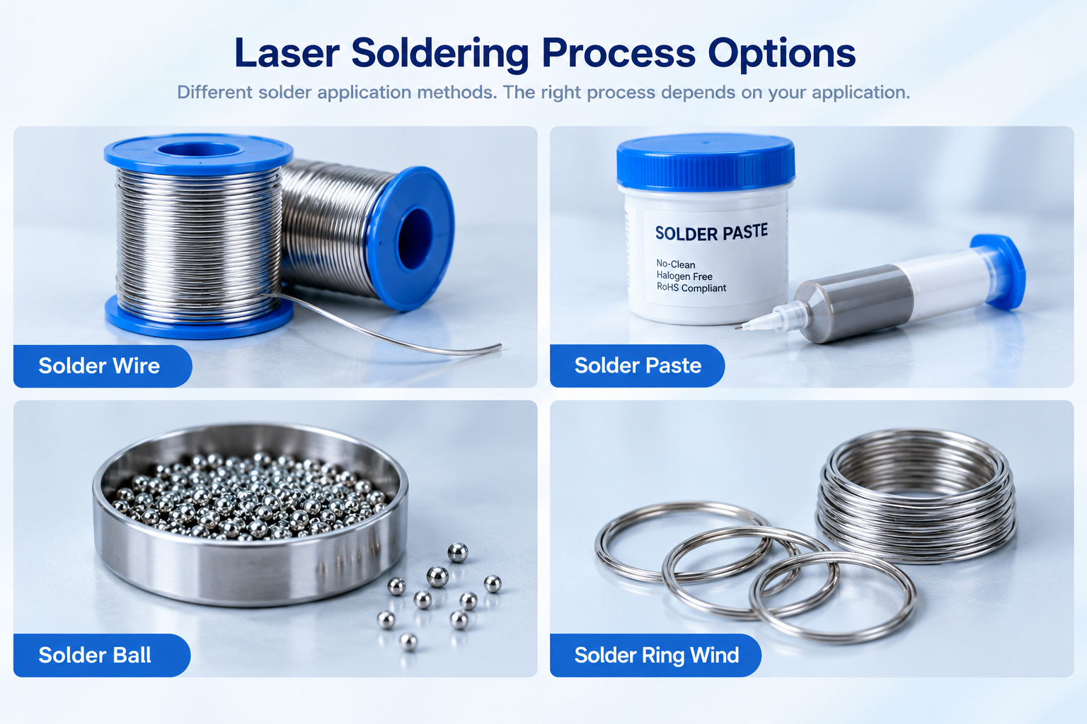
- Solder delivery. Ball, paste or wire — see the comparison below.
- Laser heating with closed-loop control. Preheat, ramp, peak dwell and cooling, each with a measured tolerance rather than a nominal setting.
- Solidification, AOI and data logging. Every joint should carry its own peak-temperature and time-above-liquidus record for traceability.
Solder Ball, Paste or Wire: Which Feed Method Fits Your Package?
The feed method sets your minimum joint size, your flux strategy and your cycle time. Choose it before you choose the machine configuration, not after.
| Feed method | Typical deposit range | Placement accuracy | Flux handling | Best-fit packages |
|---|---|---|---|---|
| Solder ball (pre-formed) | 0.15–1.0 mm diameter | ±25–50 µm | Requires flux dot or N₂/formic | TO-can headers, connector pins, BGA rework, sensor leads |
| Solder paste (dispensed) | 0.1–0.6 mm dot, 60–80 % metal load | ±30–60 µm | Flux in vehicle; residue control needed | Die attach, QFN/BGA rework, fine-pitch lead frames |
| Solder wire (with or without flux core) | 0.1–0.5 mm diameter | ±50–80 µm | Flux-cored or fluxless with N₂ | Through-hole pins, shield frames, wire-to-pad joints |
Ball feeding gives the tightest volume repeatability and is the default for pre-form-critical joints. Paste is more forgiving on irregular pad geometry but adds a stencil-free dispensing tolerance and a residue-cleanliness question. Wire is the most flexible for mixed joint sizes on one panel, at the cost of the widest volume spread — expect ±10 % volume variation versus ±3–5 % for ball.
How Do You Set and Validate the Closed-Loop Temperature Profile?
Set the profile against the alloy, then verify it at the joint — not at the laser head. Diode sources in the 915–976 nm range are typical, with a 0.6–3 mm spot and 10–150 W delivered power depending on joint mass.
| Alloy | Liquidus | Target peak at joint | Time above liquidus | Notes |
|---|---|---|---|---|
| SAC305 | 217 °C | 235–250 °C | 0.5–2 s | Ramp 100–200 °C/s; preheat 120–150 °C |
| Sn63Pb37 | 183 °C | 200–215 °C | 0.5–1.5 s | Legacy and high-reliability assemblies |
| AuSn 80/20 | 280 °C | 320–340 °C | 1–3 s | Die attach and optical packages; needs fast ramp and tight overshoot control |
Validation procedure: instrument a production-representative joint with a 0.1 mm K-type thermocouple or cross-check the integrated pyrometer against it, then confirm agreement within ±5–8 °C. Run a peak-temperature study across at least 30 joints and 3 substrate warpage conditions. Set the closed-loop controller to abort on overshoot greater than 15 °C above target, and log the measured curve per joint. A profile that only holds on a flat, room-temperature coupon will fail on a warped, preheated panel.
What Defects Appear and How Do You Troubleshoot Them?
| Symptom | Likely cause | Corrective action |
|---|---|---|
| Cold joint / dull, incomplete fillet | Peak temperature too low or time above liquidus under 0.3 s | Raise peak 10 °C or extend dwell 0.3 s; re-check pyrometer emissivity calibration |
| Solder balling / spatter | Ramp too fast for the flux vehicle, or moisture in the paste | Add a 100–150 °C preheat step; verify paste thaw and open-time limits |
| Voids above 10 % by X-ray | Flux outgassing trapped under the joint, or contaminated pad | Switch to N₂ shielding below 1000 ppm O₂, reduce flux volume, check pad shelf life |
| Adjacent component damage | Spot size larger than joint, or no heat-sink path modelled | Narrow the spot 20–30 %, shorten dwell, add a local shield or thermal mass balance check |
| Intermittent joint strength | Z-height variation on warped substrate | Enable per-joint height mapping; screen coplanarity at incoming inspection |
Which Acceptance Checks Qualify a Laser-Soldered Joint?
- AOI: fillet geometry, wetting angle under 90°, no bridging, no exposed pad area above 10 %.
- X-ray: void fraction under 10–15 % depending on the joint class; measure per joint area, not per package.
- Cross-section: intermetallic compound layer 1–4 µm; above 6 µm indicates an over-driven profile.
- Mechanical: shear or pull test on lot samples with a defined minimum and a Cpk target of 1.33 or better.
- Cleanliness: ionic contamination below your product’s specification limit if liquid flux is used.
- Traceability: stored profile curve and peak temperature for every joint, retrievable by serial number.
FAQ
Can laser soldering handle a full BGA array on one package? Not economically. The process is point-by-point at roughly 0.3–2 s per joint, so it fits rework, small packages, connectors and joint counts up to a few hundred. For dense arrays, oven or vapour-phase reflow remains the practical choice.
Does the laser heat damage nearby parts? With a 0.6–1.5 mm spot and 1–2 s dwell, the heat-affected zone typically stays within 1–3 mm; verify with a thermocouple on the nearest sensitive component and set an alarm limit rather than assuming.
Is flux mandatory? No. Formic acid vapour or nitrogen shielding below 1000 ppm O₂ supports fluxless soldering, which is often required for optical modules and hermetic packages where residue is unacceptable.
What throughput should I plan for? Single-head systems run about 1 joint per 0.5–2 s excluding handling; galvo scanning or multi-head configurations raise this, but always validate with your actual joint count and handling time.
How often should the profile be re-validated? After any change to alloy lot, flux type, substrate finish or nozzle/optics, and on a scheduled basis using the thermocouple cross-check described above.
If you share your package type, joint count and alloy, our application team can map these parameters onto a specific system configuration for your line.