



Inline AOI for laser solder joints typically combines multi-angle 2D color imaging with 3D height measurement — laser triangulation or fringe projection — at a single station, because laser-reflowed joints are small, hig…
Inline AOI for laser solder joints typically combines multi-angle 2D color imaging with 3D height measurement — laser triangulation or fringe projection — at a single station, because laser-reflowed joints are small, highly specular, and have steep, short fillets that neither 2D nor 3D alone can qualify reliably. The inspection program is built from a golden board with per-joint windows on height, solder area/volume, and reflectance, then validated by attribute GR&R and cross-section correlation before release to production. For most automotive-electronics and semiconductor-packaging lines, that combination holds false calls in the 500–2000 ppm range while catching non-wet, insufficient, and excess-solder conditions at cycle times of 8–25 s per board.
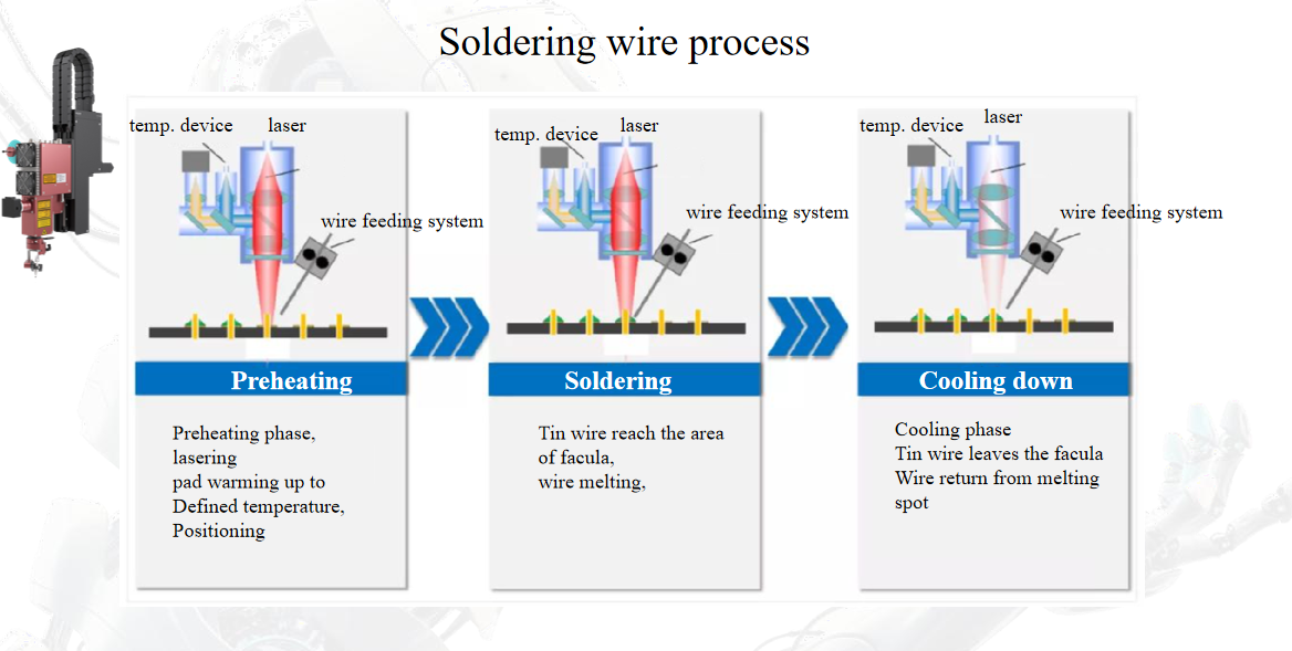
Why do laser solder joints need a different AOI setup than reflow oven joints?
Laser soldering delivers energy into a very small spot with a tight heat-affected zone, and the resulting joint geometry differs from a convection-reflowed joint in ways that directly change what the camera sees:
- Short, steep fillets and low standoff. A laser-formed fillet may rise 40–70° from the pad in under 0.3 mm of horizontal run. Side-looking illumination that works on a long reflow fillet leaves a shadow band that reads as insufficient solder.
- High specularity. With little flux residue and a fast solidification, the surface behaves almost like a mirror. A single dome light produces a blown-out highlight that saturates the sensor and hides the fillet toe — the exact region where non-wet shows up.
- Small joint count, high value per joint. Laser soldering is usually applied to a handful of critical joints (sensor terminals, connector pins, shield attach points, fine-pitch pads). Escape risk per joint matters more than throughput per board, so inspection sensitivity is weighted toward recall, not speed.
- Heat-sensitive neighbours. AOI must be non-contact and must not require board reflow or thermal cycling to reveal the joint; optical methods only.
- Disturbed or cold joints are optical, not dimensional. A joint that solidified while the laser was still ramping looks dimensionally correct. Grainy, matte, or rippled surface texture is often the only visible signature, which is why texture/gloss features matter as much as height.
Which inline AOI methods fit post-solder inspection of laser joints?
Most production lines standardise on a hybrid head. The table below compares the methods you will actually be offered, and what each contributes to a laser-soldering line.
| Method | What it measures | Typical capability | Best at catching | Practical limitation |
|---|---|---|---|---|
| 2D multi-angle color (8–16 sector RGB + low-angle dark field) | Reflectance, color, area, presence, bridging | 5–15 µm/pixel; 0.3–1.0 s per FOV | Missing solder, bridging, spatter, offset, polarity | Saturated by specular fillets; no height data |
| Coaxial / telecentric top light | Planarity, coplanarity, flat-pad detection | Telecentric distortion <0.1% | Non-wet (flat, unwetted pad), tombstoning, missing ball | Blind to steep fillet flanks |
| 3D laser triangulation | Height profile, fillet slope, volume | Z repeatability ±1–3 µm; range 0–5 mm | Insufficient/excess solder, void-driven collapse, coplanarity | Shadowing on one side; needs two-way scan |
| 3D fringe projection (phase shift) | Full-field height map | Z accuracy ±3–8 µm; 0.5–2 s per FOV | Volume and shape on multiple joints in one shot | Sensitive to vibration and to mirror surfaces |
| X-ray (AXI, where the joint is hidden) | Internal voiding, barrel fill | 5–15 µm resolution | Voids under BGA or through-hole joints | Slow, capital-intensive; not a substitute for surface AOI |
Two rules of thumb from line experience: use 3D height as the primary gate and 2D intensity as the secondary gate on specular joints, and never buy a 2D-only system for laser-soldered fine-pitch work unless every joint is visible from directly above with no flank geometry.
How should the inspection recipe and acceptance criteria be set?
Build the recipe joint-by-joint, not board-wide. For each laser-soldered joint, define a region of interest from the CAD/pad centroid, then set windows from a golden board population of at least 30 known-good, cross-section-verified boards.
| Recipe parameter | Practical starting point | Adjustment direction |
|---|---|---|
| Pixel resolution | 5–10 µm/pixel for ≤0.4 mm pitch; 10–15 µm/pixel for connectors | Finer for small solder balls; coarser to recover cycle time |
| Height window per joint | Golden mean ±3σ, floor at 60–70% of nominal fillet height | Tighten only after GR&R is confirmed |
| Fillet slope / volume | ≥25° average slope; volume ≥70% of nominal | Primary discriminator for insufficient solder |
| Reflectance / texture score | Window from golden population; enable gloss feature | Catches cold and disturbed joints |
| Minimum detectable defect | Solder ball ≥100 µm at 10 µm/pixel | Do not go below 80 µm without ROI masking |
| Cycle time budget | 8–25 s per board, matched to line takt | Reduce FOV count before reducing resolution |
Acceptance checks before sign-off: an attribute GR&R with three operators, two trials, and 30 boards should reach kappa ≥0.75; a variables GR&R on height should land under 20% (ideally under 10%); and 20 joints per board type should be cross-sectioned to confirm that what the system calls “good” is metallurgically good. Re-run a five-joint destructive audit hourly during ramp-up and daily afterwards.
What do the common failure symptoms mean, and how are they fixed?
- False calls clustered on the shiny fillets. Reduce coaxial gain, add cross-polarisation or a depolarising diffuser, and widen the intensity window while keeping the 3D height window tight. If the calls persist, switch the joint to height-only gating and use 2D only for presence.
- Escapes of non-wet joints. Usually a lighting geometry problem: the pad is flat and unwetted but reads as a dull fillet. Add a telecentric top-light channel and a “flat-pad” classifier, and check that the ROI actually covers the fillet toe.
- Height readings drifting across a shift. Thermal drift in the sensor head. Verify with a certified step block every four hours, enable temperature compensation, and check that the conveyor does not flex under the head.
- Small spatter missed. Lower the blob threshold to 80–100 µm and add ROI masks over connector cavities and shield edges so the extra sensitivity does not drown the line in false calls.
- Cold/disturbed joints passing. The laser reflow profile, not the AOI, is the root cause. Enable the texture/gloss feature, log per-joint energy and pulse timing, and correlate AOI rejects against laser parameters before widening any window.
- Voids under a BGA or through-hole joint. Not an AOI problem — route those joints to AXI, and keep the optical station focused on surface geometry.
How does inline AOI connect back to the laser soldering cell?
Put the AOI immediately after the soldering module, inside the same enclosure or on a direct SMEMA/HERMES handshake, so that a joint is measured within seconds of solidification and board tracking is unambiguous. Feed per-joint results back through CFX or the line MES: height and volume trends per joint are the earliest indicator that a laser power level, focus offset, or wire/ball feed has drifted, usually several boards before a functional failure. Archive images and 3D point data per serial number for traceability, and run SPC on the two or three joints that carry the highest consequence of escape rather than on everything.
FAQ
Can a 2D AOI system inspect laser solder joints adequately?
Only for joints with an open, top-visible pad and no steep fillet — for example some through-hole pin tops. For fine-pitch or connector joints the specular highlight and flank geometry will cause both false calls and escapes; a 3D channel is the practical minimum.
What pixel resolution do I need for 0.3–0.4 mm pitch laser-soldered pads?
5–10 µm/pixel is the working range. Below 5 µm/pixel you gain little on joint geometry and lose cycle time; above 15 µm/pixel you start missing 100 µm spatter and thin fillet toes.
How do I judge whether the AOI recipe is good enough to release?
Three numbers: attribute GR&R kappa ≥0.75, height GR&R under 20%, and zero escapes across a cross-sectioned sample of 20 joints per board type. Anything else is opinion.
Should AOI reject limits be tightened when the line’s first-pass yield is already high?
No. Tighten only where an escape has a credible field-failure consequence, and re-verify GR&R after every change — over-tightened windows on specular joints typically cost more in false calls than they save in risk.
Where does X-ray fit if I already have 3D AOI?
It complements rather than replaces it: 3D AOI qualifies surface geometry and fillet shape, while AXI is reserved for internal voiding in hidden joints such as area-array or press-fit positions.
If you want help mapping these inspection criteria onto a specific laser soldering cell and joint set, our ULiLASER process team can review your board data and propose an inline configuration.