


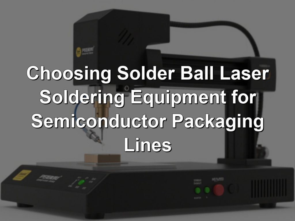
Choosing solder ball laser soldering equipment for a semiconductor packaging line comes down to matching four capabilities to your package: the ball feeding method (pre-formed ball, ball-on-paste, or ball jetting), the l…
Choosing solder ball laser soldering equipment for a semiconductor packaging line comes down to matching four capabilities to your package: the ball feeding method (pre-formed ball, ball-on-paste, or ball jetting), the laser heat source and spot geometry, closed-loop temperature control fast enough for a 1–3 second joint, and inline vision plus AOI that can verify a 0.2 mm sphere at production speed. The right system is the one whose process window you can document with a DOE on your actual die, substrate and warpage before purchase — not the one with the highest stated wattage.
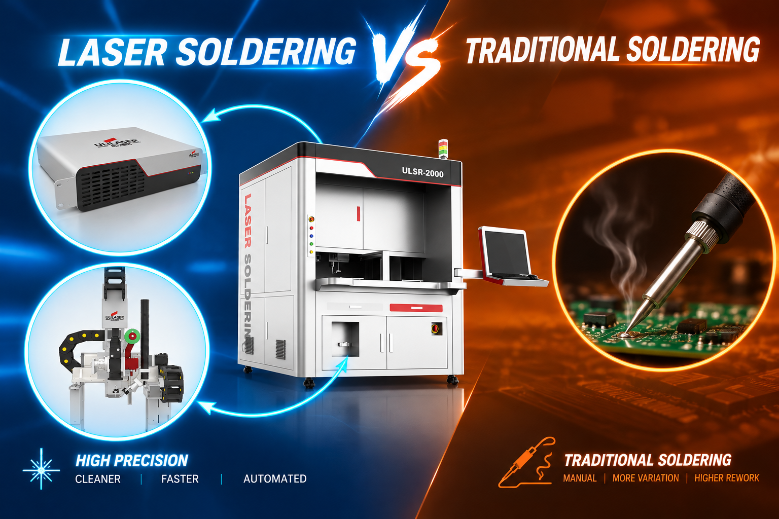
What must a solder ball laser soldering system actually do on a packaging line?
A laser soldering system for semiconductor packaging is not a reflow oven with a beam substituted for a heater. It performs a localized, per-joint thermal cycle, and each subsystem has to support that:
- Ball feed and placement: vacuum nozzle pick-and-place of pre-formed spheres, ball-on-paste dispensing, or consistent ball jetting, with ball presence and position confirmed before the laser fires.
- CCD vision alignment: coaxial or off-axis imaging that locates the pad or bump site and corrects the stage or galvo offset, typically to ±20–30 µm at 3σ for ball diameters below 0.4 mm.
- Laser heat source: diode or fiber delivery shaped to a 0.3–2.0 mm spot, with power stability adequate to hold joint-to-joint temperature within a few degrees.
- Closed-loop temperature control: non-contact pyrometry or equivalent feedback sampling at 1–10 kHz, so the controller ramps, holds and terminates the pulse on measured temperature rather than on a fixed time.
- Atmosphere control: localized nitrogen shroud keeping oxygen below roughly 1000 ppm at the joint, which is what allows low-residue or flux-free processes.
- Post-solder AOI and data: inspection for ball presence, offset, collapse height and sphere geometry, plus traceability records per joint for downstream quality systems.
If any one of these is weak, the machine becomes an operator-dependent tool rather than a process. Vision without temperature feedback produces cold joints on warped parts; temperature feedback without reliable ball presence produces intermittent opens that pass AOI and fail at final test.
Which specifications should you compare side by side?
Ask every supplier to fill the same table with values measured on a demo, not catalogue maxima. The ranges below reflect what is realistic for packaging-scale work.
| Parameter | Typical range for packaging work | What to verify on the demo |
|---|---|---|
| Solder ball diameter | 0.15–0.76 mm (extendable to 1.0 mm) | Feed repeatability and singulation at the smallest size you will run |
| Placement accuracy | ±20–30 µm (3σ) | Capability study on your pad pitch, not on a glass coupon |
| Laser wavelength / type | ~915–980 nm diode; ~1064 nm fiber | Absorption match to your solder alloy and pad finish |
| Spot diameter | 0.3–2.0 mm, adjustable | Beam profile flatness; edge spill onto adjacent joints |
| Laser power | 30–150 W at the work plane | Headroom at your required ramp rate, measured with a power meter |
| Temperature control | Closed loop, ±5 °C at hold; 1–10 kHz sampling | Emissivity calibration routine and re-calibration interval |
| Ramp / hold | 100–200 °C/s ramp; 1–3 s above liquidus | Actual joint profile from a thermal test die or fine thermocouple |
| Nitrogen purity at joint | <1000 ppm O₂ | Measured with an oxygen analyser at the nozzle, not at the regulator |
| Cycle time | 0.3–1.5 s per joint; 3–8 s per device | Including vision, ball feed, heating and AOI — end to end |
| AOI resolution | ≤5 µm/pixel for sub-0.3 mm balls | Detection of 10% ball offset and incipient void indications |
Compare on the smallest ball and tightest pitch in your product roadmap, not on the largest. Systems that look comfortable at 0.5 mm often lose feed reliability and temperature repeatability at 0.2 mm, and that is exactly where packaging programmes are heading.
How do you match the laser source and ball feeding method to your package?
Heat source. Diode sources in the 915–980 nm band couple efficiently into tin-based solders and are straightforward to shape into small, uniform spots, which suits 0.2–0.4 mm balls on fine-pitch substrates. Fiber delivery at ~1064 nm offers tighter focusing and longer working distance, useful when the joint sits in a cavity or under a stiffener. Whichever you choose, ask for the beam profile and for the power stability over an 8-hour run — drift of a few percent is enough to shift voiding behaviour at the end of a shift.
Feeding method. Pre-formed ball with a thin flux film gives the most predictable collapse and is the default for BGA and WLCSP rework and assembly. Ball-on-paste trades some collapse predictability for better self-alignment on uneven pads. Ball jetting removes placement mechanics entirely and can be faster on high-joint-count devices, but you must confirm the jetting consistency at your smallest diameter and that the AOI can still resolve sphere geometry after impact.
Force and coplanarity. Substrate warpage across a panel can exceed 50 µm. Look for closed-loop z-axis force control in the 0.5–2 N range with position feedback, so the head follows the surface instead of pressing through it. This single feature explains most of the difference between a system that runs unattended and one that needs an operator watching every panel.
What acceptance tests should you run before signing off?
Run a structured DOE on your own product: vary laser power, dwell time and nitrogen flow across at least three levels each, then evaluate joints with cross-section, X-ray and mechanical testing. A practical acceptance set:
- Temperature profile verification: thermocouple or thermal test die on three representative joints per device; confirm peak 235–250 °C for SAC305 and time above liquidus within your declared window.
- Voiding: X-ray or CT; set a limit appropriate to your die area — single-digit percentage by area is a common target for power and RF devices, with tighter limits for thermal pads.
- Intermetallic thickness: cross-section at 1–3 µm after the declared thermal excursion; excessive IMC signals an over-long hold.
- Ball shear and pull: per joint, with a defined minimum and a Cpk target across at least 30 joints per condition.
- Position and collapse consistency: measure ball height and offset across a full panel to expose stage or vision drift.
- Throughput and OEE run: four hours minimum, unscheduled stops counted, to see whether ball jams and vision false-rejects are acceptable.
Document the window you validated and make sure the machine can lock it with passwords and log every deviation. That record is what your quality system will lean on later.
What do common failure symptoms tell you?
| Symptom | Likely cause | First corrective step |
|---|---|---|
| Cold joint, dull fillet, ball not collapsed | Pyrometer reading low due to emissivity drift or spot larger than joint | Re-run emissivity calibration; verify spot size against ball diameter |
| Excess voids, spatter around the joint | Ramp too fast driving flux volatiles out late; oxygen ingress | Reduce ramp below 150 °C/s; measure O₂ at the nozzle and raise flow |
| Ball offset or tombstoning | Vision fiducial error, or uneven wetting from pad contamination | Re-teach fiducials; check pad finish and storage conditions |
| Intermittent missing ball | Vacuum nozzle wear or blocked jetting orifice | Inspect nozzle under magnification; shorten cleaning interval |
| Joint-to-joint variation across a panel | Warpage without force control; focal drift | Enable z-axis force following; verify focus offset compensation |
| Adjacent joint reflow or solder wicking | Spot too large, or dwell exceeding the thermal isolation of the site | Reduce spot diameter and dwell; check beam edge sharpness |
FAQ
Can solder ball laser soldering replace reflow for wafer-level packages?
For localized joints, thin or heat-sensitive substrates, and mixed-technology assemblies, yes — it limits total thermal exposure to the joint rather than the whole device. For high-joint-count devices where every ball must be formed in one pass, oven reflow remains more economical. Many lines use laser soldering for the joints where reflow cannot meet the thermal budget.
What is the smallest solder ball these systems handle reliably?
Around 0.15 mm is achievable in production with well-maintained nozzles and vision at 3–5 µm/pixel; 0.2–0.3 mm is the comfortable band for high-yield, low-maintenance operation. Below 0.2 mm, feed reliability and AOI resolution become the limiting factors rather than the laser.
How is oxidation controlled without a full flux load?
A localized nitrogen shroud holding oxygen under roughly 1000 ppm at the joint, combined with a controlled ramp that lets the flux activate before liquidus. Verify with an oxygen analyser at the nozzle, since ducting leaks and nozzle wear degrade purity without any visible sign.
What cycle time is realistic per device?
Roughly 0.3–1.5 s of heating per joint plus vision, ball feed and inspection. Devices with a handful of large balls commonly run 3–8 s per unit; high-joint-count devices need parallel heads or jetting to stay competitive.
How do we handle panel warpage?
Specify closed-loop z-axis force control in the 0.5–2 N range with position feedback, then validate across your worst-case warped panel. Also check that vision focus compensation covers the same range, otherwise placement accuracy degrades even when force control works.
If you send us your ball diameter, pad pitch, substrate warpage range and target throughput, we can map them against ULiLASER system configurations and propose a demo plan built around your actual devices.